EMC concepts explained
Evaluation of EMC Emissions and Ground Techniques on 1- and 2-layer PCBs with Power Converters
Part 8: AC/DC Converter – Baseline EMC Emissions Evaluation
T

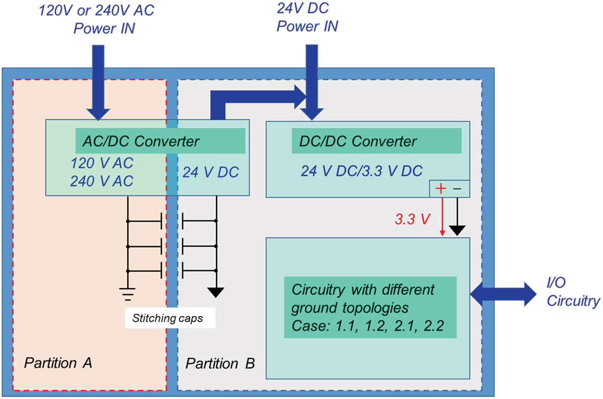
his is the eighth article in a series of articles devoted to the design, test, and EMC emissions evaluation of 1- and 2-layer PCBs that contain AC/DC and/or DC/DC converters and employ different ground techniques [1-7].

In this article, we evaluate the performance of the baseline AC/DC converter. The baseline AC/DC converter has only the components needed for functionality and does not have any specific EMC components populated. [7] This configuration will give us a view into what the conducted and radiated emissions issues will be prior to adding components and the cost to specifically address EMC issues. We present the test results from the baseline radiated and conducted emissions tests performed according to the CFR Title 47, Part 15, Subpart B, Class B.

1. Introduction
Figure 1 shows the functional blocks of the PCB assembly [1].

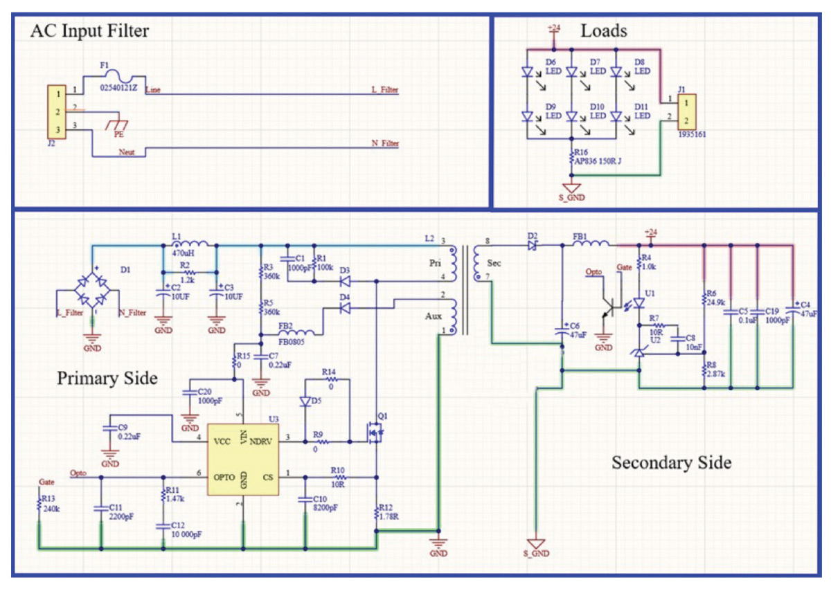
The baseline schematic for the AC/DC converter is shown in Figure 2.

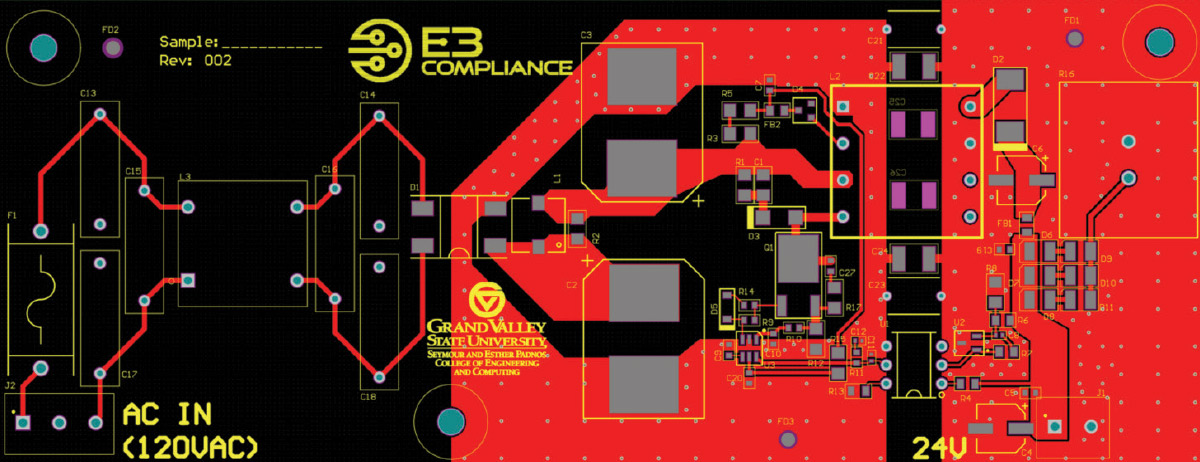
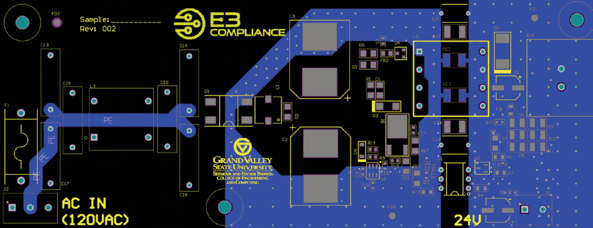
The top layer of the PCB used to create the AC/DC converter is shown in Figure 3, while the bottom layer is shown in Figure 4.

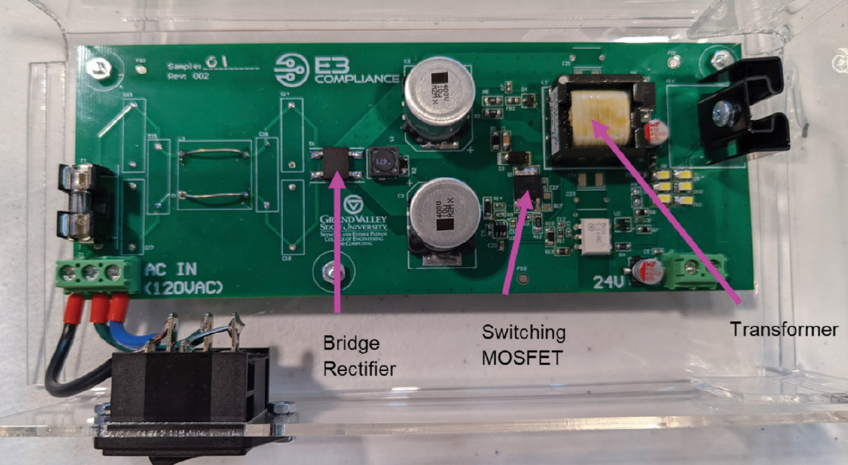
Figure 5 shows the baseline AC/DC PCB converter populated with the baseline components.

This article is organized as follows. Section 2 presents the baseline radiated emissions test results. In Section 3, the baseline conducted emissions results are shown. Section 4 addresses the content of the next article.

Top-level schematic – functional blocks
Figure 1: Top-level schematic – functional blocks
AC/DC converter baseline schematic
Figure 2: AC/DC converter baseline schematic (EMC components removed)
Top layer of the PCB
Figure 3: Top layer of the PCB
Bottom layer of the PCB
Figure 4: Bottom layer of the PCB
Baseline AC/DC converter PCB with components
Figure 5: Baseline AC/DC converter PCB with components
2. Radiated Emissions Test Results
The AC/DC converter was tested according to CFR Title 47, Part 15, Subpart B, Class B.

A legend for the radiated emissions plot is shown in Figure 6.

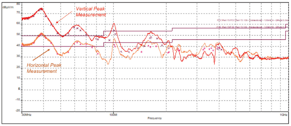
Radiated emissions measurements were made using a biconical antenna from 30 MHz – 300 MHz and a log-periodic antenna from 300 MHz – 1 GHz.

Radiated emissions legend
Figure 6: Radiated emissions legend
The measurements were taken with the DUT at four different positions (angles) with each side of the PCB facing the antenna. We only present the results for the zero-degree angle (AC inlet facing the antenna) as this angle resulted in the highest emissions. Figure 7 shows the results from 30 MHz – 1 GHz.

As shown in Figure 7, there are numerous failures in the biconical range (30 MHz – 300 MHz). These will be investigated in the next article.

Radiated emissions results in the frequency range 30 MHz
Figure 7: Radiated emissions results in the frequency range 30 MHz – 1 GHz
The failing emissions are considered broadband noise and come primarily from the switching circuitry and magnetics. At these frequencies, the harness length is the most likely antenna where common mode emissions conduct and re-radiate effectively. Reducing these emissions will most likely involve filtering, using snubber circuits, and tuning stitching capacitance between the SGND and GND.
3. Conducted Emissions Test Results
A legend for the conducted emissions plots is shown in Figure 8.

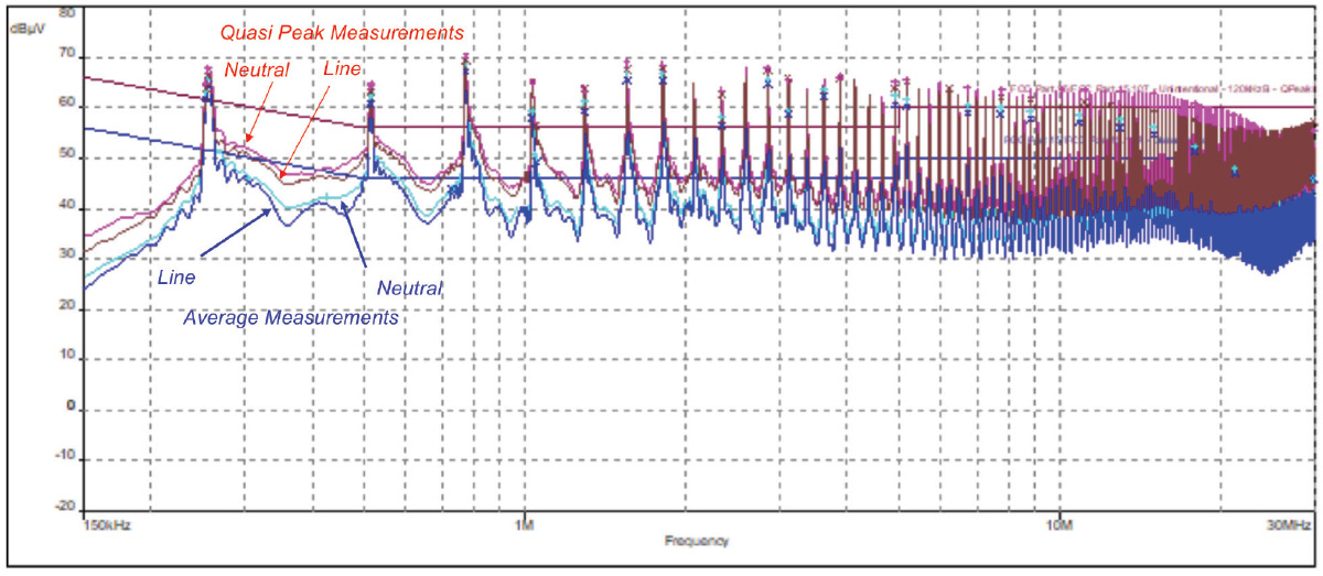
The test results on both the line and neutral, in the frequency range of 150 kHz – 30 MHz, are shown in Figure 9.

The conducted emissions results show multiple failures up to the frequency of 20 MHz. The failures are comprised of the fundamental switching frequency (~ 270 kHz) and the subsequent harmonics. Reducing these emissions will most likely involve front-end filtering components such as a common mode choke, Y-capacitors, and X-capacitors. These will be investigated in the next article.

Conducted emission results legend
Figure 8: Conducted emission results legend
Conducted emission test results 150 kHz - 30 MHz
Figure 9: Conducted emission test results 150 kHz – 30 MHz
4. Future Work
The next article will be devoted to the evaluation of EMC countermeasures to address the radiated and conducted emissions non-conformities. The article will address each test result and the impact of the optional EMC components.
References
  1. Adamczyk, B., Mee, S., Koeller, N, “Evaluation of EMC Emissions and Ground Techniques on 1- and 2-layer PCBs with Power Converters – Part 1: Top-Level Description of the Design Problem,” In Compliance Magazine, May 2021.
  2. Adamczyk, B., Mee, S., Koeller, N, “Evaluation of EMC Emissions and Ground Techniques on 1- and 2-layer PCBs with Power Converters – Part 2: DC/DC Converter Design with EMC Considerations,” In Compliance Magazine, June 2021.
  3. Adamczyk, B., Mee, S., Koeller, N, “Evaluation of EMC Emissions and Ground Techniques on 1- and 2-layer PCBs with Power Converters – Part 3: DC/DC Converter – Baseline EMC Emissions Evaluations,” In Compliance Magazine, July 2021.
  4. Adamczyk, B., Mee, S., Koeller, N, “Evaluation of EMC Emissions and Ground Techniques on 1- and 2-layer PCBs with Power Converters – Part 4: DC/DC Converter – EMC Countermeasures- Radiated Emissions Results,” In Compliance Magazine, August 2021.
  5. Adamczyk, B., Mee, S., Koeller, N, Evaluation of EMC Emissions and Ground Techniques on 1- and 2-layer PCBs with Power Converters – Part 5: DC/DC Converter – EMC Countermeasures – Conducted Emissions Results,” In Compliance Magazine, October 2021.
  6. Adamczyk, B., Mee, S., Koeller, N, “Evaluation of EMC Emissions and Ground Techniques on 1- and 2-layer PCBs with Power Converters – Part 6: PCB Layout Considerations,” In Compliance Magazine, November 2021.
  7. Adamczyk, B., Mee, S., Koeller, N, “Evaluation of EMC Emissions and Ground Techniques on 1- and 2-layer PCBs with Power Converters – Part 7: AC/DC Converter Design with EMC Considerations,” In Compliance Magazine, December 2021.
Share this story:
Bogdan Adamczyk headshot
Dr. Bogdan Adamczyk is professor and director of the EMC Center at Grand Valley State University (http://www.gvsu.edu/emccenter) where he regularly teaches EMC certificate courses for industry. He is an iNARTE certified EMC Master Design Engineer. Prof. Adamczyk is the author of the textbook “Foundations of Electromagnetic Compatibility with Practical Applications” (Wiley, 2017) and the upcoming textbook “Principles of Electromagnetic Compatibility with Laboratory Exercises” (Wiley 2022). He can be reached at adamczyb@gvsu.edu.
Scott Mee smiling in a professional headshot
Scott Mee is a co-founder and owner at E3 Compliance which specializes in EMC & SIPI design, simulation, pre-compliance testing and diagnostics. He has published and presented numerous articles and papers on EMC. He is an iNARTE certified EMC Engineer and Master EMC Design Engineer. Scott participates in the industrial collaboration with GVSU at the EMC Center. He can be reached at scott@e3compliance.com.
Nick Koeller smiling in a professional headshot
Nick Koeller is an EMC Engineer at E3 Compliance which specializes in EMC & SIPI design, simulation, pre-compliance testing and diagnostics. He received his B.S.E in Electrical Engineering from Grand Valley State University and is currently pursuing his M.S.E in Electrical and Computer Engineering at GVSU. Nick participates in the industrial collaboration with GVSU at the EMC Center. He can be reached at nick@e3compliance.com.