hot topics in ESD
The Dilemma Between Customers and Suppliers on EOS Failures
Bridging the Gap using tAMR
Never-ending EOS Customer Returns
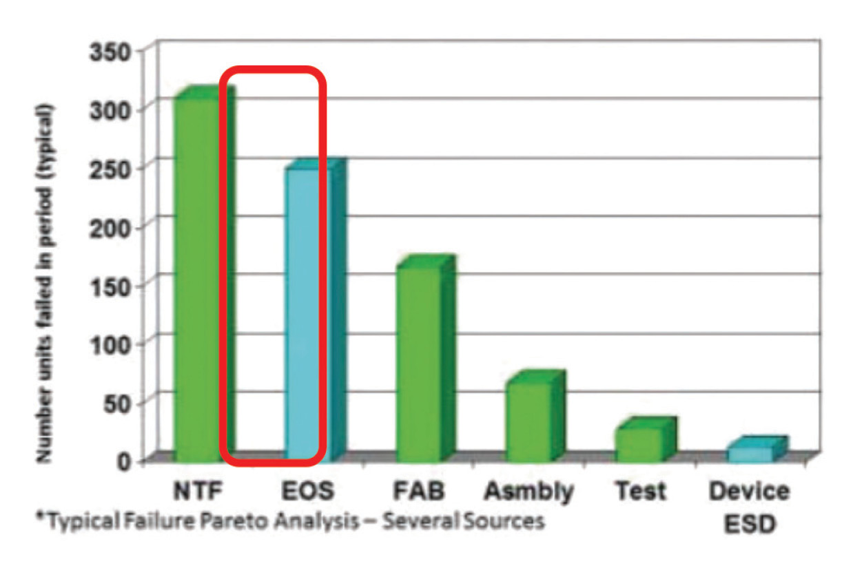
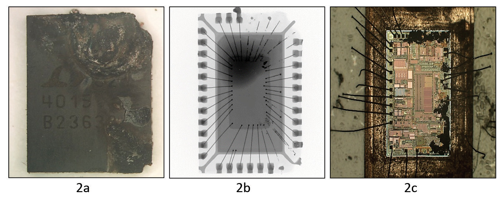
During the last four decades, damage to devices from electrical overstress (EOS) has confounded both IC suppliers and customers. The Industry Council on ESD Target Levels investigated numerous EOS root causes and established a white paper on the subject, JEP174 [1]. The original motivation came after observing that the most common and top Pareto item as indicated in the failure Pareto analysis in Figure 1 for semiconductor component field returns is Electrical Over Stress (EOS) failures. More often, NTF, or no trouble found, has been attributed to EOS failures as well. One of the major reliability challenges is a failure that appears to be electrically induced physical damage (now commonly known as EIPD) as shown in optical, X-ray, and decapsulated images in Figures 2a, 2b, and 2c. The failures were produced with no prior indications, leaving customers wondering what might have caused it, when it might have occurred, and how it might have happened. A thorough analysis including but not limited to curve tracing, electrical characterization, optical and x-ray microscopy, and decapsulation is often required to prove that failures are in fact caused by electrical overstress. Failure analysis reports from the industry indicate failures can range from damage to the package to fused and melted wire bond to melting or burning of the stacked material that is hidden in the semiconductor die.
Figure 1: Failure Pareto showing EOS as the top item (Danglemayer Assoc & Semitracks Inc)
If this is any indication of the problem that several end customers face on a day-to-day basis, it is evident that EOS failures are a clear and present danger to semiconductor component reliability. However, it has been elusive when it comes to the identification of a root cause and solution. The most important question that needs to be answered is what causes semiconductor components to fail due to electrical overstress when there are protective strategies in place within the component, as well as external to it? In addition, the component datasheets have absolute maximum ratings (AMR) published that serve as a warning for system designers to pay attention to maintain the reliability of the component. However, in the white paper on EOS, it was noted that AMR does not provide the full picture.

To answer the question of what causes EOS failures, a holistic approach needs to be taken. While absolute maximum ratings (AMR) are published in product datasheets, they don’t address the limitations due to the inherent transients that the components experience due to several reasons such as inductive coupling, EMI/EMC, etc. that are typically application specific. The presence of these transients which range from Direct Current (DC) to nanosecond (ns) and their impact on component reliability are often not considered mainly because of the lack of understanding of their effects.

Figure 2: a) Crater on top of the package due to EOS, b) X-ray image showing melted bond wire, c) decapsulated image of the die showing damage on die
Effects of Transient AMR
It is more important to understand the types of signals that manifest on the pins of the integrated circuit components and the boundary conditions in the form of ratings and specifications that are in place to have a minimal impact. The absolute maximum ratings (AMR) have often been associated with DC stress limits that should not be violated to maintain product reliability. However, under certain conditions, this AMR may need to be exceeded to meet some specific applications where transients are involved. But these transients are not all the same as they will vary in duration and magnitude. For example, if the AMR was specified as 3 V, during certain field events the product or system might see up to 7 V for a few microseconds or a few milliseconds. There is a misunderstanding that the shorter the transient, the less power is delivered and hence the lower the likelihood of EOS damage. However, to understand the transient nature of AMR for all product and system applications, we must define the transient nature of AMR or what is referred to as tAMR. This can provide comprehensive insight into signal integrity aspects of a component in relation to the overall system design.
Figure 3: Effect of pulse duration on the probability of damage
Figure 3 illustrates the effect of pulse duration and the impact of immediate damage. The regions below the Maximum Operating Condition depicted as A and B are safe for all handling and applications, with region B being where the effects are understood when violated. Exceeding the absolute maximum rating or AMR is the most critical condition where the damage probability begins. The yellow curve in Figure 3 below represents this behavior and it predicts that as the stress is increased beyond this limit the probability of immediate damage goes up and eventually reaches 100%. But if there is a condition where the pulse duration is shorter in time it should take a higher level of stress to reach the same probability of immediate damage at any given stress point. As an illustration, this is shown by the blue solid curve in Figure 3; an even shorter pulse time is shown by the green solid curve. This might sound reasonable theoretically, but is this approach realistic or accurate?

The curves with less transient times do not necessarily shift in a parallel fashion as shown by the blue and green solid curves. One can envision that since the power to failure from the well-known Wunsch-Bell relation is a function of time to failure, the true shifts in these probability curves might involve a stochastic process. We can perhaps try to represent them with the dashed blue and green curves to convey that at lower stress levels the shift for transient pulses would be less compared to the shift at higher stress levels. These cannot be confirmed without detailed studies that include field relevant studies and gathering data that relate to various transient conditions and their impact on robust system designs. There are complex parameters involved such as minimum stress to create thermal damage, power to failure versus pulse widths for specific example case studies, and an understanding of statistical reliability models and the limits and regions of their applications, etc.

There have been several case studies from different applications published in Industry Council WP4 [1]. The common thread among the cases appears to be a lack of clarity on the specifications for absolute maximum rating for transient signals. It becomes even more important in high-reliability applications such as automotive, medical, and aerospace.

Transient Stress and Reliability Prediction Using Simulation
As illustrated in Figure 3, the impact of a transient pulse can be immediate or progressive degradation. EOS pulse could potentially degrade the reliability affecting the maximum stress level for a given lifetime. A maximum acceptable level of stress for critical electrical parameters like current, voltage, or power needs to be established from a Wunch-Bell relationship for short-stress conditions and a reliability model will determine the maximum stress level for longer-stress conditions. Simulation methodologies can provide valuable assistance in analyzing and understanding the transient stresses and failure mechanisms. Also, simulation can help narrow down the focus area by identifying the regions of interest on the chip/system and transient waveforms of interest. These insights can be of great help in designing more robust devices, circuits, and systems. Simulation tools and workflows provided by Ansys can be of valuable assistance in the analysis of tAMR by providing both qualitative and quantitative results.
Conclusions
In summary, a characterization method for representing transient AMRs like the one proposed in the Industry Council White Paper on tAMR needs to be considered and evaluated. The proposed method defines a safe operating area (SOA) within the derated limits of the failure threshold due to degradation mechanisms including thermal degradation. If the customer is knowledgeable and aware of the methodologies and is willing to work with the supplier in ensuring that reliability is predicted and designed into the system, it will potentially prevent field failures of semiconductor components due to electrical overstress.

As a final note, there is much to be investigated on this complicated subject of tAMR. The Industry Council on ESD Target Levels plans to publish a new extension of White Paper 4 on the subject soon.

Reference
Share this story:
Ashok Alagappan headshot
Ashok Alagappan has over 15 years of experience in the Semiconductor industry, specializing in design and manufacturing of semiconductor products. At Ansys, he is working with customers across the spectrum, from aerospace to automotive to commercial, providing expert analysis and solutions for defining and improving reliability of electronic products and Integrated Circuit (IC) components.
ESD Association logo
Founded in 1982, EOS/ESD Association, Inc. is a not for profit, professional organization, dedicated to education and furthering the technology Electrostatic Discharge (ESD) control and prevention. EOS/ESD Association, Inc. sponsors educational programs, develops ESD control and measurement standards, holds international technical symposiums, workshops, tutorials, and foster the exchange of technical information among its members and others.