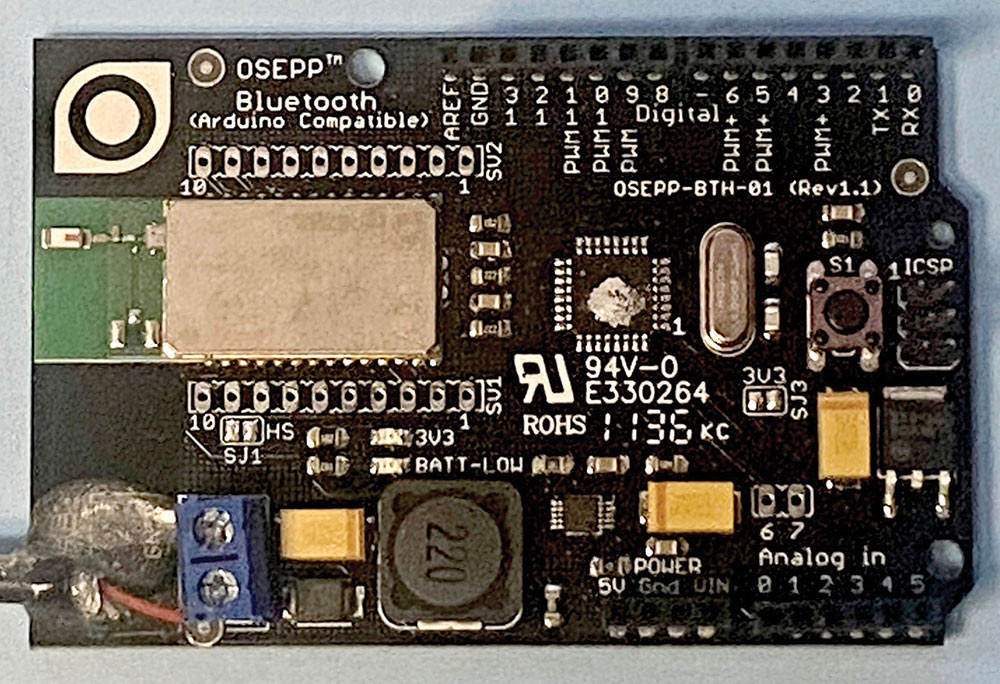
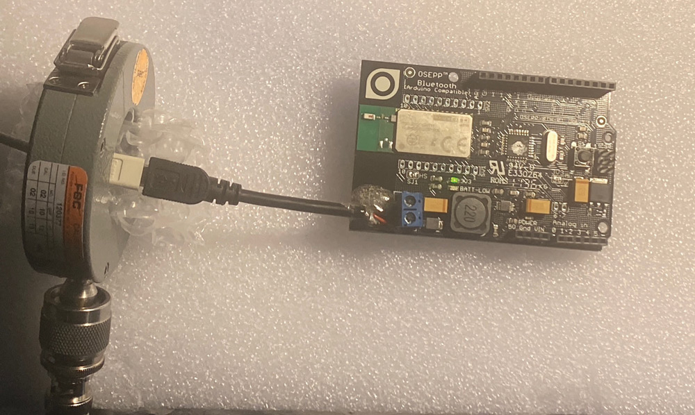
et’s use the basic tools and spectrum analyzer setup I described in the last two months and use them to characterize an actual embedded processor board based on the Arduino design. I’ll be using an “OSEPP Bluetooth” board, but you can use anything on hand or similar (Figure 1). The schematic and board layout are available in Reference 1. While most Arduino-based boards use linear regulators, I chose this board from my collection because it includes a DC-DC converter and uses a two-layer design with obvious EMC issues.

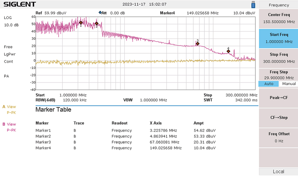
Let’s make some near field probe measurements; first on the DC-DC converter. This is easy to identify because of the large 22µH inductor at the bottom of the board. We’ll non-invasively couple to the inductor (Reference 2), which is connected to the MAX1676 boost converter. Figure 3 shows the resulting frequency domain plot. Placing the spectrum analyzer in Max Hold mode, we can see a lot of switching energy extending out to 200 MHz. You’ll notice that for each plot, I record the system noise floor (yellow trace). I also placed markers at some of the resonant peaks, which we may use in possible future analyses.
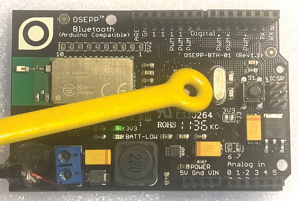
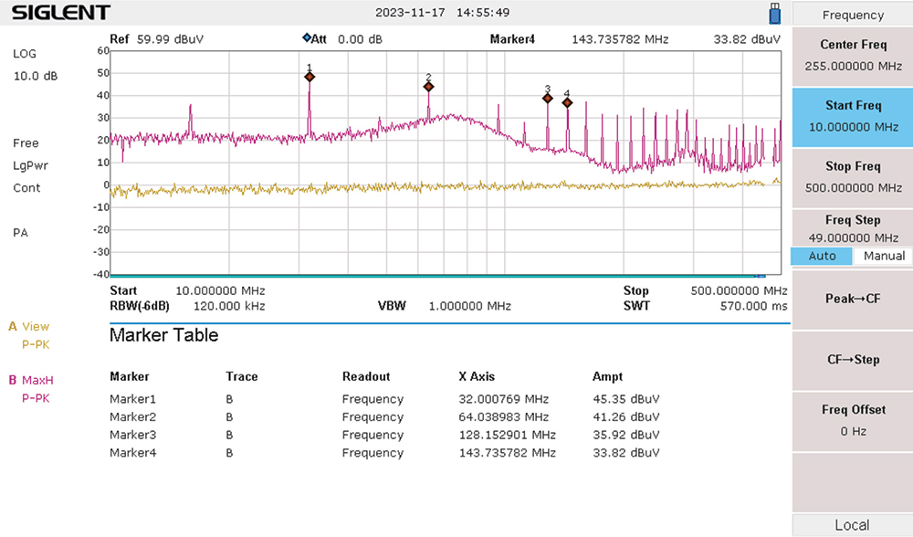
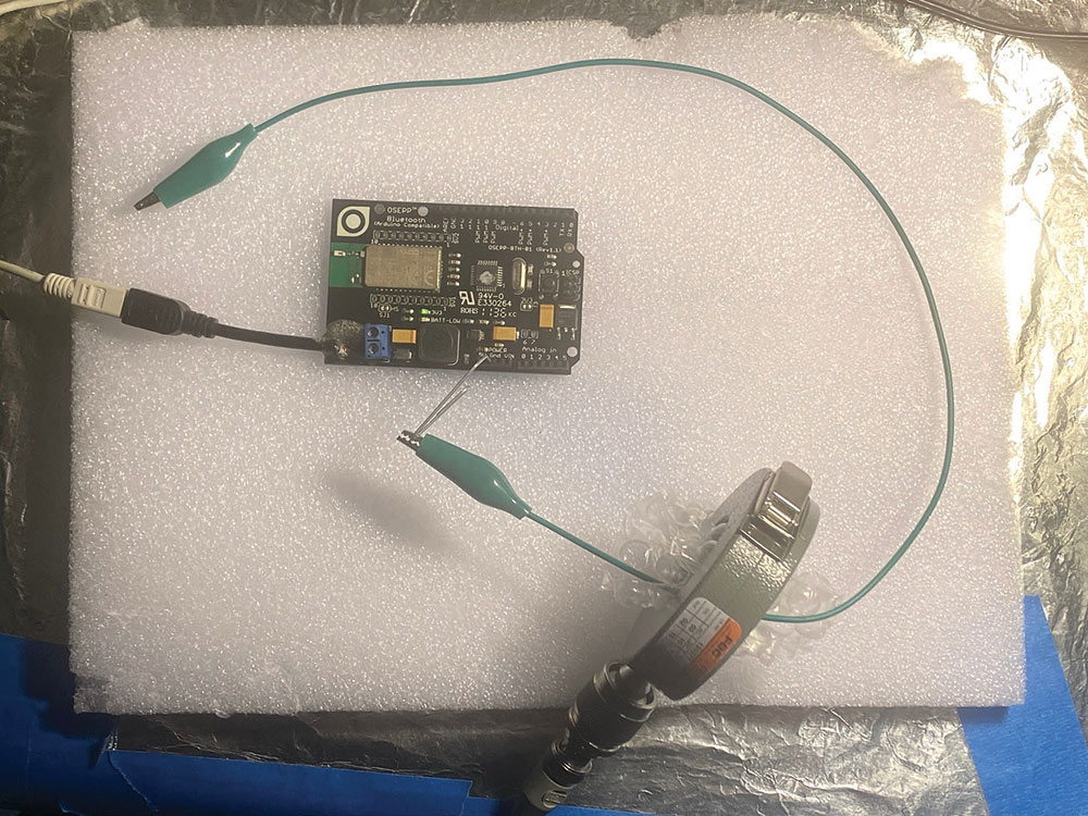
Now, let’s clamp our current probe around the DC power input cable (Figure 6). I’ve inserted some “bubble wrap” around the power cable to help isolate it from the metal case of the probe. Here, we observe very strong broadband switching noise with a 16 MHz peak (Figure 7).


Digital signals are not the result of electron flow through circuit traces but are propagated via electromagnetic waves between the circuit trace and the nearest other metal. Because we lack a solid ground return plane, these EM waves must be “trapped” between two pieces of metal at all times to propagate the signal energy from point A to point B. However, without an adjacent and solid return plane, the signal energy in the EM wave will couple to all other traces they pass by. Please refer to my PC board design series starting with Reference 4.
It’s possible to re-lay out this board with the top layer as mainly routed power and signals and then use a semi-solid return plane for the bottom layer with minimal non-critical signal routing. You’d need to be careful to avoid high-frequency traces crossing gaps in this return plane.
Many of my clients have already invested their design in a two-layer board, only to learn at the last minute that it may never pass EMC requirements. So, often, I’ll suggest keeping the current layout but simply adding two additional ground return planes as layers 2 and 3, which should be bonded together (along with all ground fill) with stitching vias in a grid pattern. Today, the cost differential between two- and four-layer boards is insignificant, so this is often the most cost-effective solution. The suggested stack-up is shown in Figure 11.

There are other design issues that would preclude me from using this particular board in a “real” product. For example, it lacks power input filtering as well as filtering or ESD protection on the I/O pins. I’d also change the I/O connectors to include optional I/O cable shields.
In future articles, we’ll be characterizing a more complex embedded computer with USB, Ethernet and HDMI ports, along with multiple DC-DC converters.
- OSEPP Bluetooth module design information
- Wyatt, “Characterize DC-DC converter EMI with near-field probes,” EDN.
- Wyatt, “Gaps in return planes – yes or no?” EDN.
- Wyatt, “Design PCBs for {low} EMI, Part 1: How signals move,” EDN.