In automotive power electronics, there is one standard that has been either implemented or adopted as part of an OEM specification for interfacing and testing modules on a power bus, and that is a class of emissions limits defined in CISPR 25, “Vehicles, boats and internal combustion engines – Radio disturbance characteristics – Limits and methods of measurement for the protection of on-board receivers.”
The purpose of CISPR 25 is to set limits to provide protection for receivers installed in a vehicle from disturbances produced by components/modules in the same vehicle, including switching power supplies, one of the biggest culprits of conducted disturbance. The standard covers frequency-dependent emission limits (in dB) and methods for test, including spectrum analyzer settings and test setup. It applies to electronics equipment and devices intended for use in vehicles or trailers.
To meet this design requirement, automotive power supply designers, including power management IC (PMIC) designers, have implemented a variety of different features in their products over the years. These features include:
- Slew rate control, where the designers can limit the slew rate of the switching signal and slow the pulse width modulation (PWM) switching speed; and
- Anti-phasic clock generation, where multiple modulators are driven out of phase with respect to each other.
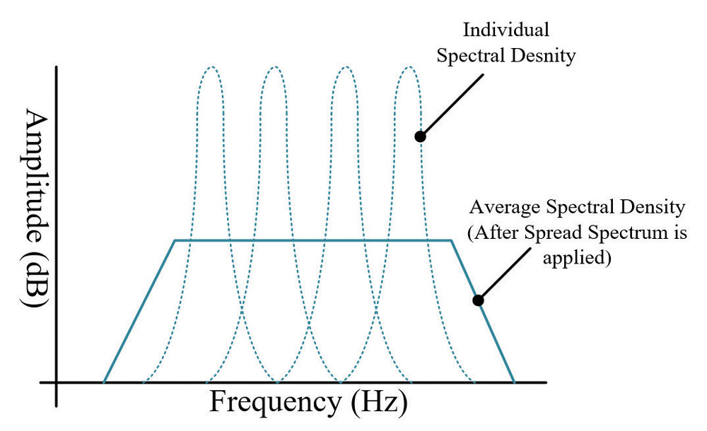
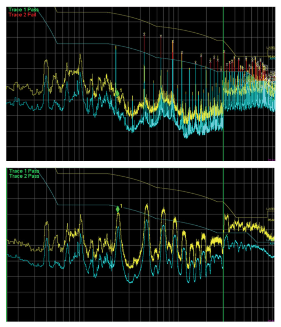
Among these, however, is a more universal concept, spread spectrum clock generation, which has been widely adopted by digital designs and implemented on many modern-day power management devices. This allows the normally impulsive energy of a clock to be “spread” out over a wider frequency range, reducing the amplitude of the conducted emission generated by the clock. An example of this is shown in Figure 1.
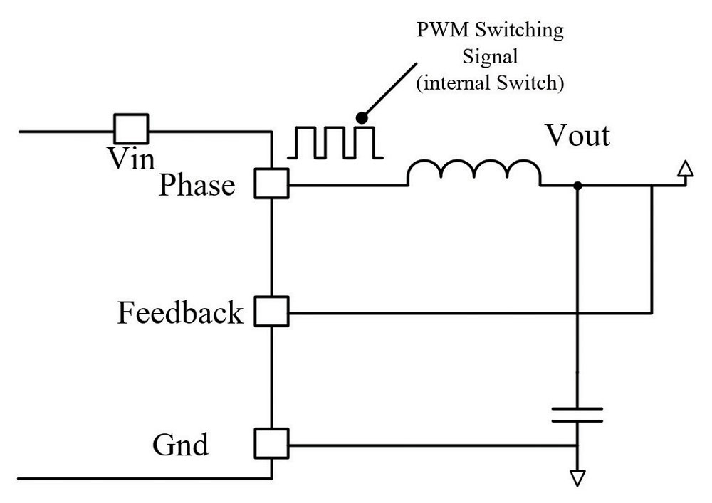
Spread spectrum modulation applies to the PWM signal coming from what is commonly called the phase node used to drive either an external or internal switch. This switching on and off through an external filter is what gives high efficiency switch mode power supplies their allure. But it’s also why they’re the main source for conduced emissions (CE).
To understand how modulating the device turns the switch on and off and how it interacts with the standards, we’ll start by giving an overview of CISPR 25 testing. Here, understanding of how the spectrum analyzer transforms a continuous time signal and represents it as a series of frequency spectra along with the proper limits is key to understanding the design of a proper spread spectrum generator. And, since this source of emissions can couple in non-predictable ways through unforeseen coupling paths, it’s important to define a proper test setup so that repeatable results can be generated when evaluating schemes.
After identifying the important testing-related aspects outlined by this standard, we’ll turn to the source of the problem itself, discuss the design goals of a spread spectrum scheme, and how it is used in a switch mode power supply. We’ll focus on tunable factors commonly found as part of the design and outline the main design goals that go into modulating the clock.
The article will offer insight in how a spread spectrum function interacts with the measurement standard and how poor design can complicate matters. The goal is to demonstrate how spread spectrum can help the modulator meet emissions limits (or unwittingly make things worse!).
When designing or evaluating a design according to CISPR 25, understanding how a continuous time signal is represented in signal spectra is key in understanding how these two topics relate to each other. In theory, spectrum can be defined as a collection of sine waves superimposed on each other in the time domain and in the frequency domain, with each sine wave operating within its own fundamental frequency.
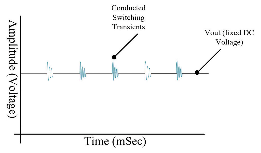
However, in reality, it’s not that simple since we often have a DC signal with switching transients superimposed on top of it, as shown in Figure 3.
In both cases, both domains help characterize the design in different ways:
- The time domain helps with functional details such as overshoot, ringing, settling time, and undershoot and is more closely related to devices functional performance.
- The frequency domain helps with regulatory and integration details, which ensures that the strength of those transient signals is within a limit that doesn’t impact neighboring electrical devices and signals. These features are more often referred to as regulatory performance.
To do this, we employ a family of devices that allow us to analyze these continuous time signals and represent them in the frequency domain, classified as signal analyzers. These devices do their job through a various combination of analog and digital circuits. This family of devices covers spectrum analyzers, EMC analyzers, vector generators, and, sometimes, even the “FFT” function on an oscilloscope.
The operating principles of these devices are similar. But to keep things simple, the focus of this section will be a swept-tuned superheterodyne measurement device, a type of spectrum analyzer that sweeps and measures a range of frequencies higher than those used for audio communications. Our goal is to understand how the frequency impacts the measurement and how the measurement process measures and captures a continuous time signal to represent it as signal spectra.
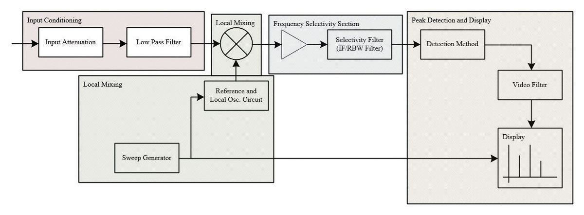
To understand why CISPR outlines not only the test setup but also the bandwidth settings, our attention needs to turn to the fundamental block diagram of how a spectrum analyzer functions. It is made up of subsystems that limit the input, mix it with a local oscillator, and then various filters and conditioning circuits that aid in the display of the signal’s spectra. An example block diagram is shown in Figure 4.
Next, we’ll go into more detail for each of the subsystems.
Input Attention
The first subsystem is the input signal conditioning circuit. This subsystem is generally made of an attenuator and often a pre-selector filter. Its focus is to ensure that the signal enters the mixer at the optimum level for measurement. An example is shown in Figure 5.
By providing input attenuation, the device ensures that the signal is free from distortion by the spectrum analyzer by limiting it to a suitable input level for the downstream circuits, thereby providing physical protection and creating a suitable noise floor.
Mixing
Next is the mixer circuit. This subsystem, often made up of more than one mixing step, synchronizes the span of the screen to the portion of the signal spectra being measured. The basis of this circuit is where the device gets its name, heterodyne, which means to mix. By mixing the input signal spectra with a local oscillator, a new signal is created based on the local oscillator which includes not only the original signal but the harmonics which need to be filtered.
The Intermediate Filter (IF) and Gain
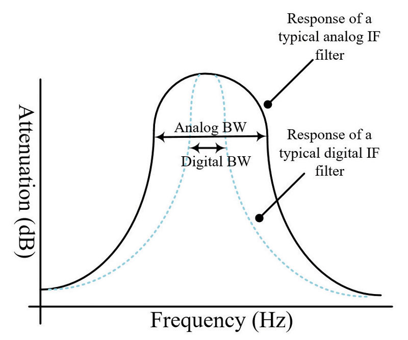
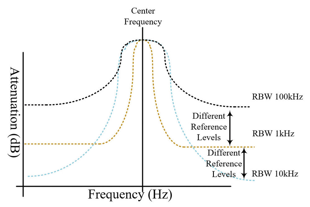
After mixing, we need to filter and adjust the positions of the signals on the display without impacting the signal level at the input mixer. As the IF gain level is changed, the value of the references changes in relation to that. Next is the filter itself, which exists to create resolvability between signals of unequal amplitude. The filter exists as a bandpass filter of configurable bandwidth called the resolution bandwidth (RBW) that determines selectability. An example of this discrimination is shown in Figure 6.
What was once an analog bandpass filter with poor selectivity and wide bandwidth now exists as a digital filter with the ability to decrease the bandwidth of the filter.
The Detector and Video Bandwidth Filter
After the input signal passes through the IF filter, it goes through a detector that outputs a signal, the amplitude of which is proportional to the power passing through the IF filter. This detector once existed as a pure analog part (modeled as a diode) which detected only the peaks. With the advent of digital spectrum analyzers, more examples include:
- Negative/positive peak
- Normal
- Average
- Quasi peak, or
- Sample

The difference in how the detector operates is based on the specification being followed. For example, positive peak is often the default on most devices as it ensures that no sinusoid is missed in the display (it displays every peak frequency scanned). But in comparison with other modes, it may not give a good representation of random noise in the system when testing broad band noise from a motor since it only detects the maximum value at each frequency and ignores the “randomness” of the brushed motor noise. The detection type is generally matched to the application.
Lastly, before the detector displays the output, the input signal is passed through another filter, the video filter. Unlike the IF, this filter is usually matched to the span and display settings of the analyzer. Its purpose is to smooth the noise inherent to the signal being measured, and its bandwidth is called the video bandwidth, or VBW. The narrower the bandwidth, the less noise there is in the output signal. But, once again, the narrower the bandwidth, the longer the sweep time and overall impact on the amplitude of the signal being measured.
Tunable Parameters
The main tunable parameters of a spectrum analyzer are:
- The input attenuation setting, which while often set can be tuned to create a more optimum baseline in which to view the signal spectra;
- The frequency span, which impacts both how much of the signal spectrum you’re seeing and the sweep time;
- The bandwidths, which impact how much of the spectrum is being represented on the screen; and
- How the envelope of the signal is detected.
To find out how the shape of these filters relate to the representation of the signal, we’ll investigate how their bandwidth can impact the amplitude, and how it relates to CISPR requirements.
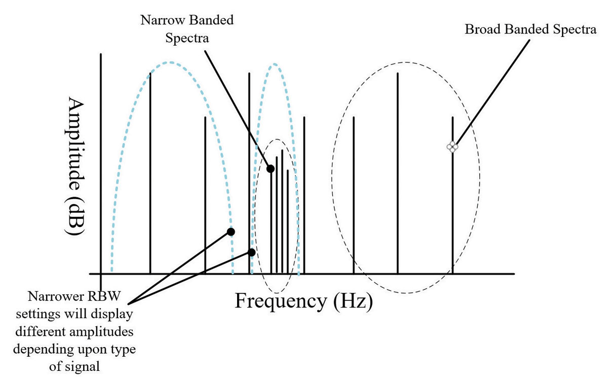
The primary purpose of the RBW filters that exist after the mixing stage is to resolve adjacent signals of different frequency representations. The key term here is “adjacent signals,” which plays an important role in addressing how the spectrum analyzer can be configured to properly represent the signal. We do that by first defining two different types of signals usually measured in a conducted emissions test:
- Narrow banded signals, usually caused by a grouping of signals inside of a narrow band of frequency spectra. Usually, these signals have a defined frequency and well-defined amplitude and change based on the defined bandwidth; and
- Broad banded signals, signals which show no change in maximum defined amplitude with changes in spectrum analyzer bandwidth.
As the RBW filter is modified and the signal amplitude changes, the definition of the signal becomes more apparent. An example of the selectivity is shown in Figure 9.
By decreasing the bandwidth of the filter, we decrease the amount of signal being measured. This helps in isolating narrow banded signals, but the result might not be representative of broad banded signals.
A clock can fit into the definition of narrow banded signals when the fundamental frequency has jitter or is frequency modulated. In general, they are usually represented as a fundamental frequency and their associated harmonics at multiples of the base frequency that scale based on the fundamental frequency. For example, if we have a base clock switching at 2MHz, we’ll see a spectral line at 2MHz, 4MHz, 6MHz, and so on, with their spacing being a function of the base switching frequency. Great care must be taken when considering the RBW settings for the following reasons:
- If set too high, the RBW will not be able to distinguish between adjacent signals (or harmonics), and you may end up capturing more than the frequency of interest.
- If set too low, the RBW will not be able to capture all the spectral lines of interest.
Ideally, you want to set the RBW as narrow as possible to capture the frequency of interest. However, doing so comes with an increase in sweep time. Luckily, to accurately measure the signal from the LISN, CISPR 25 defines the bandwidth and scan time based on the frequency range of interest depending upon the detection method. Some examples are shown in Table 1 on page 18.
It’s important to take note that the full definition of a Class 5 measurement in CISPR 25 defines the following as a function of the frequency range or spanning range:
- A noise floor, which is impacted by the input attenuator of the analyzer;
- The resolution bandwidth; and
- The sweep time, a direct function of how much the span is.
Next, we’ll discuss how this relates to proper design of a spread spectrum generator when choosing exactly how close the frequencies hop between and the shape of the slope of the clock.
Spread spectrum techniques are abundant in clocking and are used to deliberately spread the frequency of the clock in the frequency domain, resulting in a wider bandwidth with lower amplitude. Its main advantage to the system is that, by reducing the source of conducted emissions (i.e., the PWM clock), the peak emission is spread over a larger frequency range.
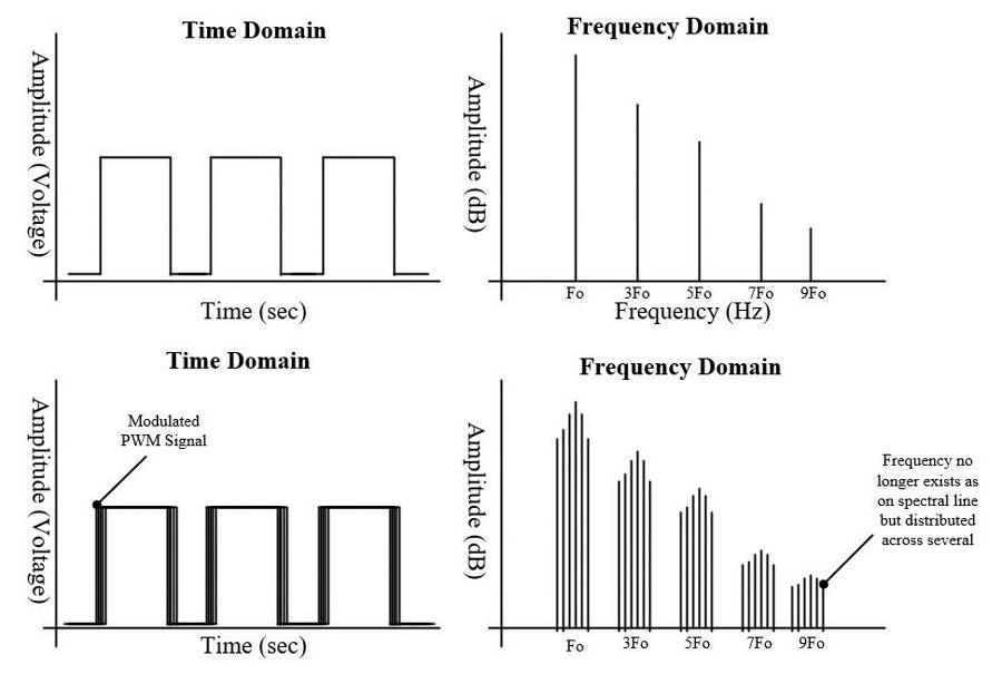
A physical demonstration of this modulation scheme is demonstrated in Figure 10. It compares the measurements before and after clocking modulation is turned on, represented in both the time and frequency domain.
We characterize the amount of modulation as a percentage of the targeted clock signal, typically measured in the kHz range. For example, if we take a 1MHz switching signal and modulate it by 1%, the frequency range would dither between 990kHz and 1.05MHz, resulting in a signal spectrum that no longer spends all its time at the fundamental frequency of 1MHz. In a power regulator, the two ways to set this dithering are frequently either:
- An external resistor which, when coupled with a current source, produces a voltage that translates to a percentage; or,
- In more advanced applications, via one-time programmable fuse options where both the frequency dithering percentage and shape of the clock is chosen internally to the device.
Next, we’ll discuss design decisions as they pertain to a spread spectrum modulation scheme and then relate it to the RBW of the spectrum analyzer.
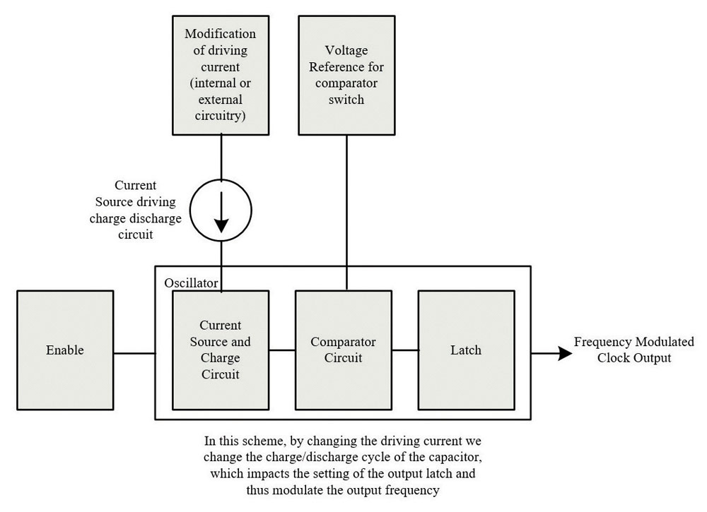
At its core, the spread spectrum modulator is a frequency modulation scheme that controls the jitter of the PWM in the time domain by algorithmically bouncing around the fundamental clock frequency. The result of this scheme in the frequency domain is a spectral line that no longer exists at just one frequency but instead at multiple, similar frequencies.
The result is a reduction in both the peak and overall average energy at the targeted switching frequency (Fsw). The diagram shown in Figure 11 demonstrates an algorithmic flow chart representative of a frequency hopping spread spectrum generator.
And while the most optimal dither is of debate, it is often targeted to the application, there exists a combination of parameters that can be tuned for a specific situation. The options pertain specifically to the dithering or jumping of the fundamental PWM frequency. Some popular design decisions that impact the dithering amount are:
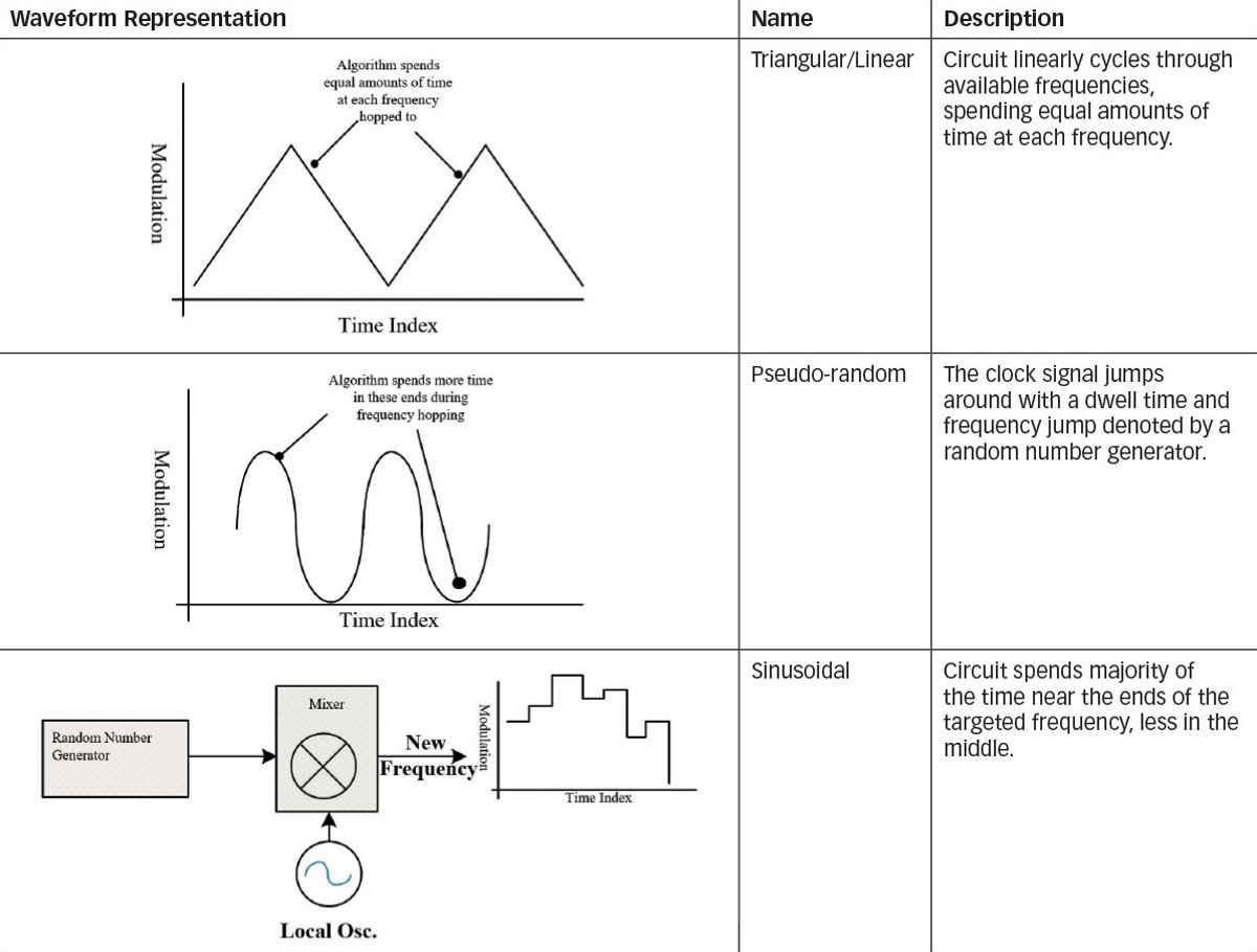
- Controlling the frequency being hopped through pseudo-random frequency hopping or a specific modulation scheme. Instead of linearly running through the list of allowable frequencies, it hops between them with a random number generator, according to an algorithm or external circuit.
Table 2 demonstrates this concept with different schemes. This is basically understood as how long the clock spends at each frequency between the minimum and maximum.
- Controlling the dwell time, or how long the clock frequency spends at each frequency that is hopped to. This can also be random. In general, a smaller dwell time means a more rapid repeating of each frequency hop, but too long or too short of a dwell time impacts the average noise measurement.
- Controlling the spacing of the frequency hops. We want to make sure that, as the frequency dithers between the maximum allowable limits, the hops are far enough apart to be distinguishable. The important thing to note here is that the dithering can be either continuous or digital (an example is shown in Figure 12).
And, in a complex mixed-signal design, there will often be more than one implementation selectable via fuse or register that will allow for evaluation of the best implementation. The overall goal is to reduce both the:
- Peak amplitude of the fundamental frequency of the PWM clock; and
- The average power associated with each harmonic.
An example is shown in Figure 12 of a before and after spread spectrum, with both the average and peak signals taken.
Now that we’ve introduced how RBW impacts the measurement taken and how a spread spectrum modulation scheme impacts the frequency spectrum, we can put the two together to understand how they impact the measurement and obtain some design goals.
As we covered in the previous section, we’re able to shape the signal spectra of the PWM signal by choosing the modulation scheme. This results in the amplitude of each of these spectral lines being impacted by choosing parameters that impact the dwell time and the frequency hopping. If the RBW parameter is overlaid on top of what the signal spectra looks like, some design goals are quickly realized based on the interaction of measurement and function. Specifically:
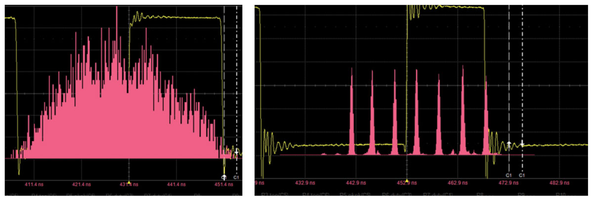
- The tightness of the SS frequency hopping must not be so close together that two or more frequencies fit under the same RBW filter. By creating a narrow-banded clock spread, the result would be an increase of signal spectra at that frequency instead of a decrease.
- The bandwidth of the dithered signal as it relates to the RBW is extremely important as it relates to the spread of the energy being measured. If the dithered signal has a very narrow bandwidth, the peak amplitude is likely to be high. Spreading the bandwidth to take advantage of the full RBW of the spectrum analyzer will reduce the average of the harmonic being measured at each RBW interval.
By following these design goals, we can thereby control the peak and average emissions. This also means that a spread spectrum generator that produces very tight discrete frequency bands may not always be the best design approach when it comes to reducing emissions, depending upon the application and design goal.
To demonstrate this, an example is shown in Figure 13 of a spread spectrum clock in the frequency domain in two different designs. The first design has a spectrum that is spread in such a way that the spectral content is wider than the implemented RBW. The second keeps the frequency tight (violating one of our design goals).
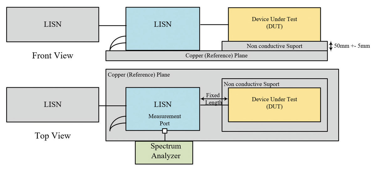
Now that we’ve covered signal spectra, how to measure it, and what spread spectrum modulation is, we’ll define components of an average test setup defined in CISPR 25. This test setup can be used to create repeatable measurements from algorithm to algorithm to evaluate different algorithms selected for spreading the clock frequency.
Lastly, to evaluate a design using spread spectrum against CISPR 25 or any recognized standard, we introduce a fixed test setup which consists of:
- A line impedance stabilization network (LISN) or current probe. This device provides a measurement for noise from the device, tuned to the frequency of interest;
- A spectrum analyzer that, when properly configured, provides the measurement capabilities; and
- Copper table or transverse electromagnetic wave (TEM) cell. Both these devices allow for a means of isolation from the environment, with the TEM cell traditionally is used for radiated emissions testing and the copper table for conducted emissions.
This test setup, along with fixed cable lengths, shown in Figure 14, demonstrates a traditional way in how conducted emissions (CE) are measured. It’s important to remember, however, to refer to the published standard for an exact setup.
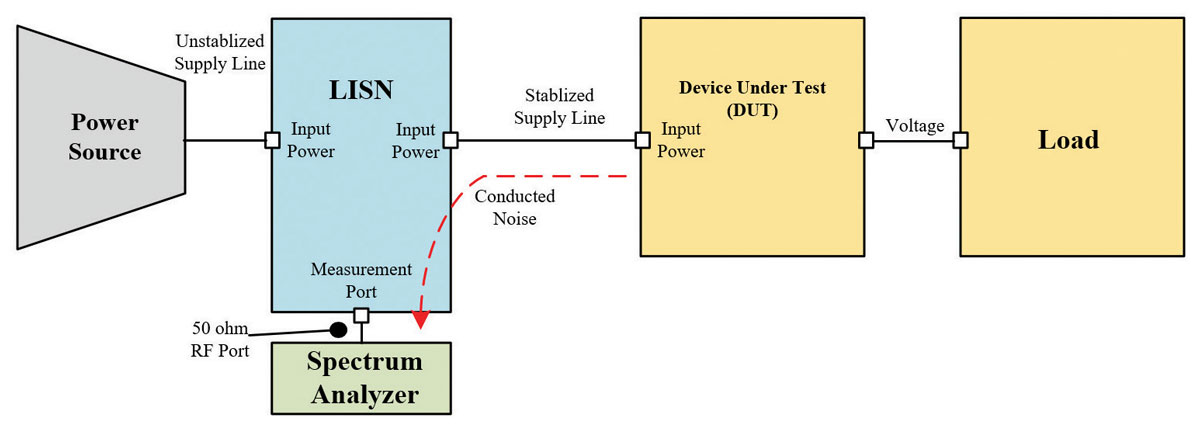
The LISN stabilizes the line impedance, isolating the device from external interference, and provides a measurement port at the specific frequency range of test. Figure 15 demonstrates where the emission from the device can be measured using both a LISN as a measurement device and to stabilize the line impedance.
As demonstrated in these figures, it’s not always the power lines that are measured. Depending upon the application, the measurement could include:
- The entirety or portion of a wiring harness
- Positive or return voltage lines
- Control lines
- The entirety or portion of a wiring harness
- Positive or return voltage lines
- Control lines
or any combination of these elements. It’s important to remember that the ambient noise of the test setup needs to be a significant dB below the intended reference level to receive an accurate measurement. This ambient noise is often taken prior to putting the device under test (DUT) inside of the TEM cell or on the board.
When designing or evaluating a design to meet the conducted emissions regulatory requirements found in CISPR 25, it’s paramount to have an understanding of the frequency spectra and the measurement of that spectra.
By tracing the conversion process from the continuous time measurement to the frequency domain, we can understand how bandwidth limits and scan times impact the measurement. Next, by understanding how frequency modulation via a spread spectrum algorithm impacts the spectral content, we can overlay these two theories to create design goals. Through these design goals and creating a fixed environment in which to test, proper evaluation can be done on various spread spectrum schemes such that they are able to stay under the various limits imposed by CISPR.
With this understanding, the next time you need to evaluate or design for such a requirement, you have a more complete understanding of how to look at a signal in both the time and frequency domain, and how the spectrum analyzer can be configured to give you the most accurate measurement needed to evaluate your design.

