his article presents a simple method of estimating the parasitics of the three passive circuit components (R, L, C). First, the non-ideal model of each component is presented, followed by the network analyzer measurements. The component (approximate) model serves as the basis for analytical calculations leading to the values of the parasitics.
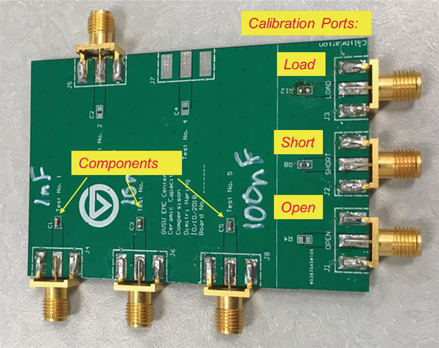
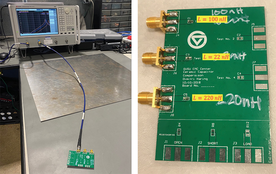
The PCB used in this study, [1], is shown in Figure 1.
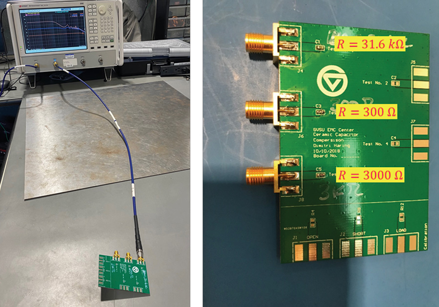
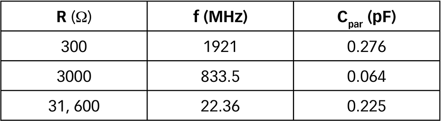
Resistor impedance curves are shown in Figure 4.
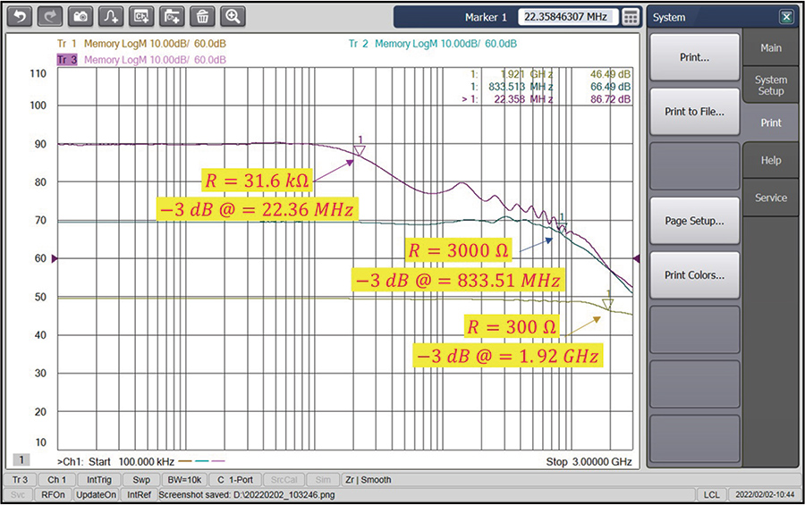
Each curve shows a 3-dB point corresponding the frequency (shown in Figure 1):
The resulting parasitic capacitance values for the three resistors are shown in Table 1.
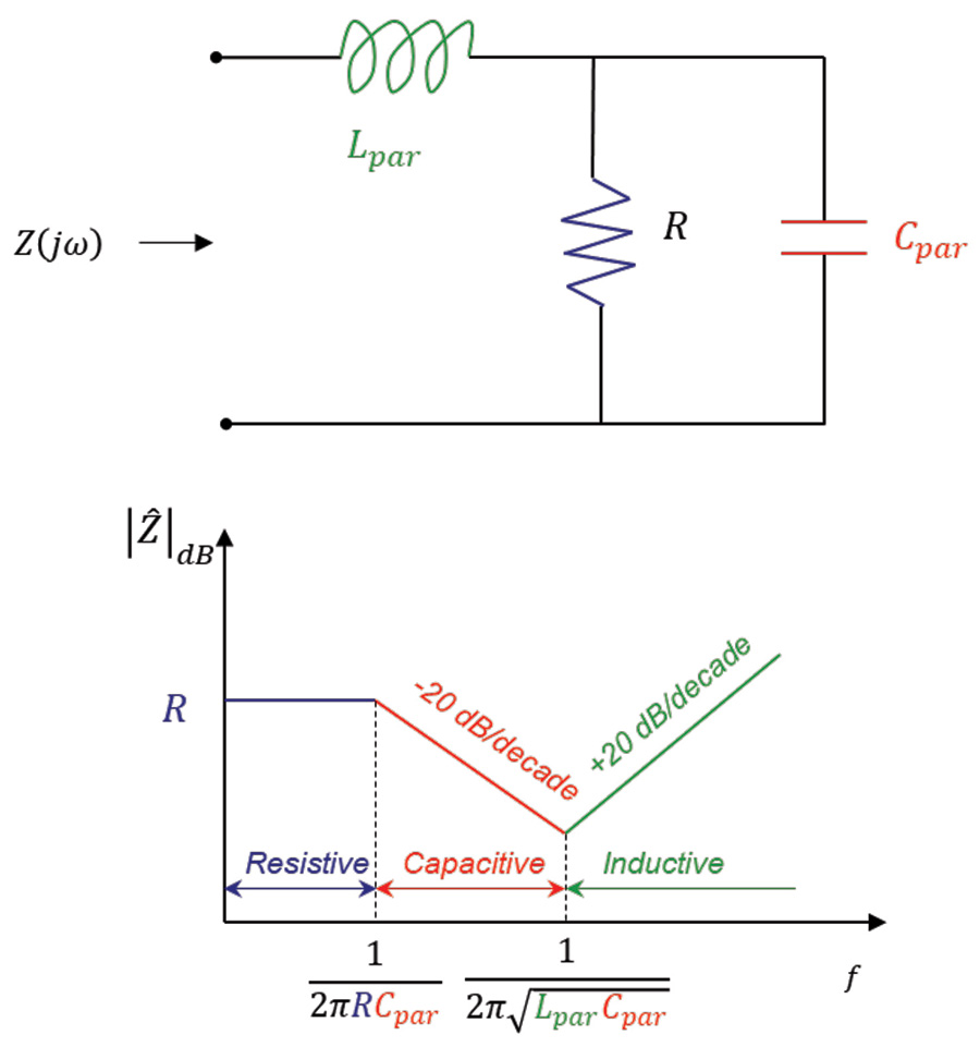
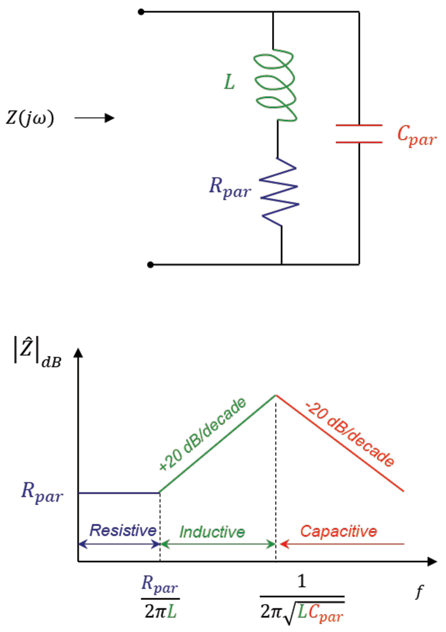
Circuit model and the impedance vs. frequency curve (straight-line approximation) for a capacitor and its parasitics (with no traces attached) are shown in Figure 5 [1,2].
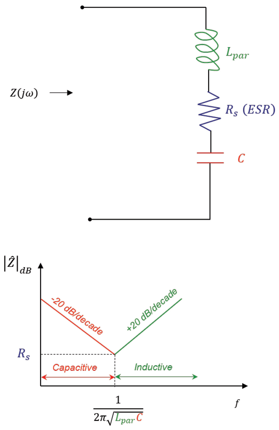
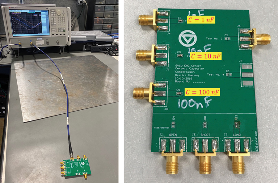
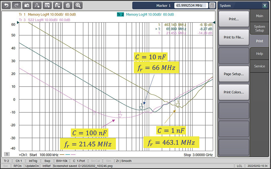
Figure 7: Capacitor impedance curves
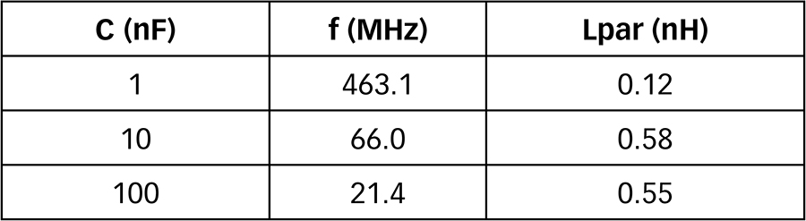
The resulting parasitic inductance values for the three capacitors are shown in Table 2.
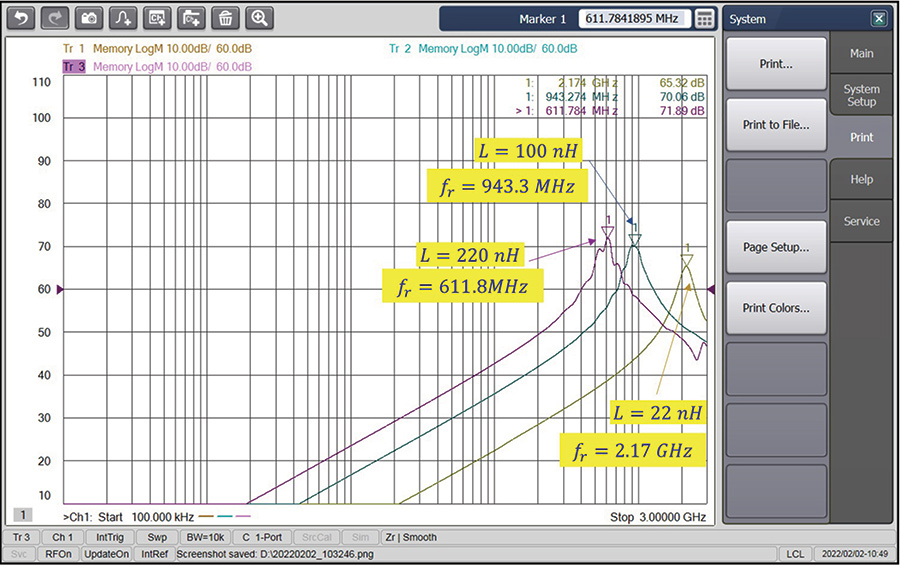
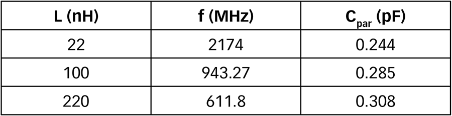
Inductor impedance curves are shown in Figure 10.
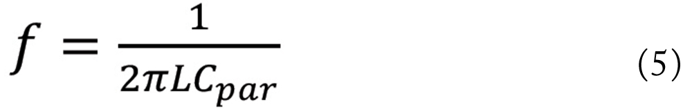
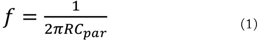
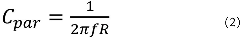
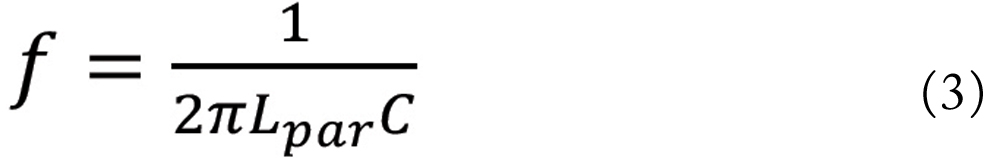
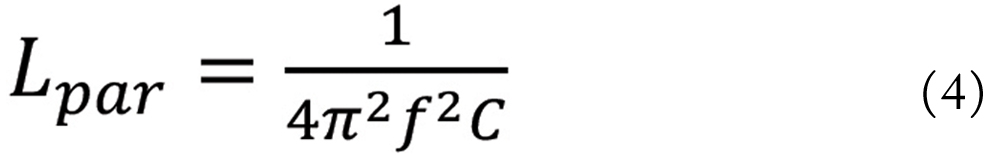
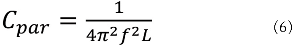
From Equation 3 the parasitic inductance can be obtained as:
- Haring, D., designer of the PCB used in this study
- https://www.mwrf.com/technologies/test-measurement/article/21849791/copper-mountain-technologies-make-accurate-impedance-measurements-using-a-vna
- https://www.clarke.com.au/pdf/CMT_Accurate_Measurements_VNA.pdf
- https://passive-components.eu/accurately-measure-ceramic-capacitors-by-extending-vna-range
- https://www.w0qe.com/Measuring_High_Z_with_VNA.html
- Adamczyk, B., Teune, J., “Impedance of the Four Passive Circuit Components: R, L, C, and a PCB Trace,” In Compliance Magazine, January 2019.
- Adamczyk, B., “Basic Bode Plots in EMC Applications – Part II – Examples”, In Compliance Magazine, May 2019.