Part 1: Fundamental Concepts
his is the first of two articles devoted to an eye diagram. In this article, the fundamental definitions and concepts are presented. The next article will show the impact of driver, receiver, and interconnect properties on signal quality using data eye and data eye mask concepts while evaluating several different HDMI cables.
An eye diagram is basically an infinite persisted overlay of all bits captured by an oscilloscope to show when bits are valid. This provides a composite picture of the overall quality of a system’s physical layer characteristics. This picture covers all possible combinations of variations affecting the signal: amplitude, timing uncertainties, and infrequent signal anomalies.
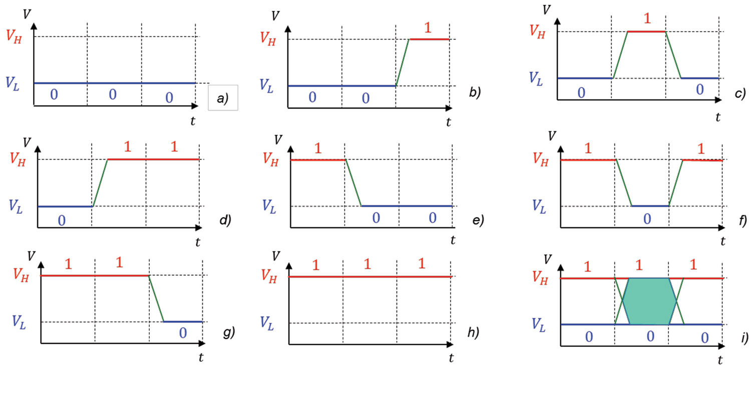
The eye diagram is created by superimposing successive bit sequences of the data. Consider all possible 3-bit sequences shown in Figures 1a through 1h.
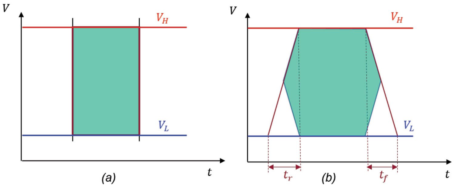
It should be noted that the data sequences in Figure 1 and Figure 2a are shown as straight lines; the actual data stream looks like the one shown in Figure 2b.
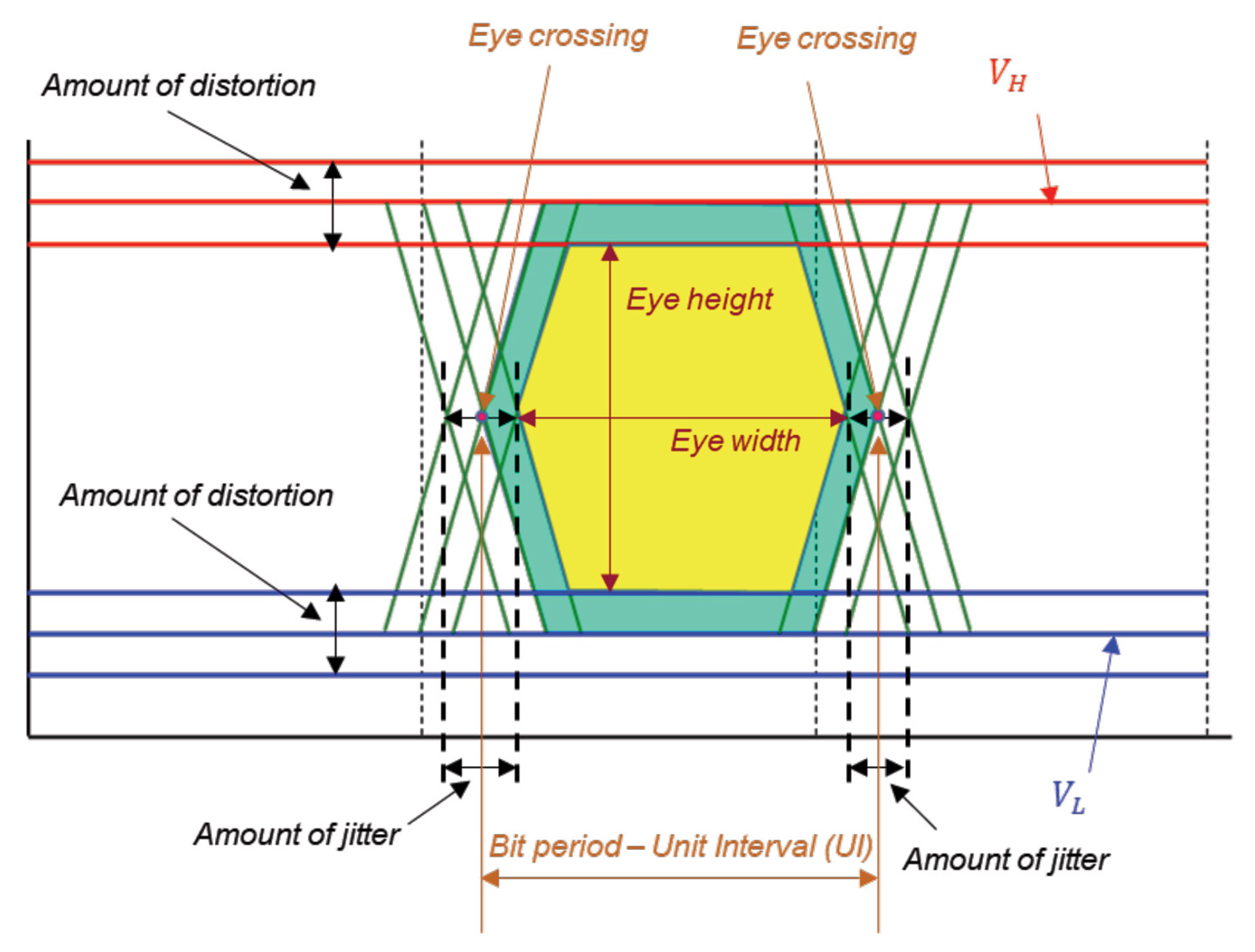
An even more realistic signal would exhibit some degree of amplitude and rise/fall time variation. These amplitude and time variations give rise to several parameters associated with an eye diagram, as shown in Figure 4 on page 50.
Note that the eye area has been reduced. The eye crossing in Figure 4 is often referred to as a zero crossing since the data used for an eye diagram creation is usually transmitted as a differential pair signal.
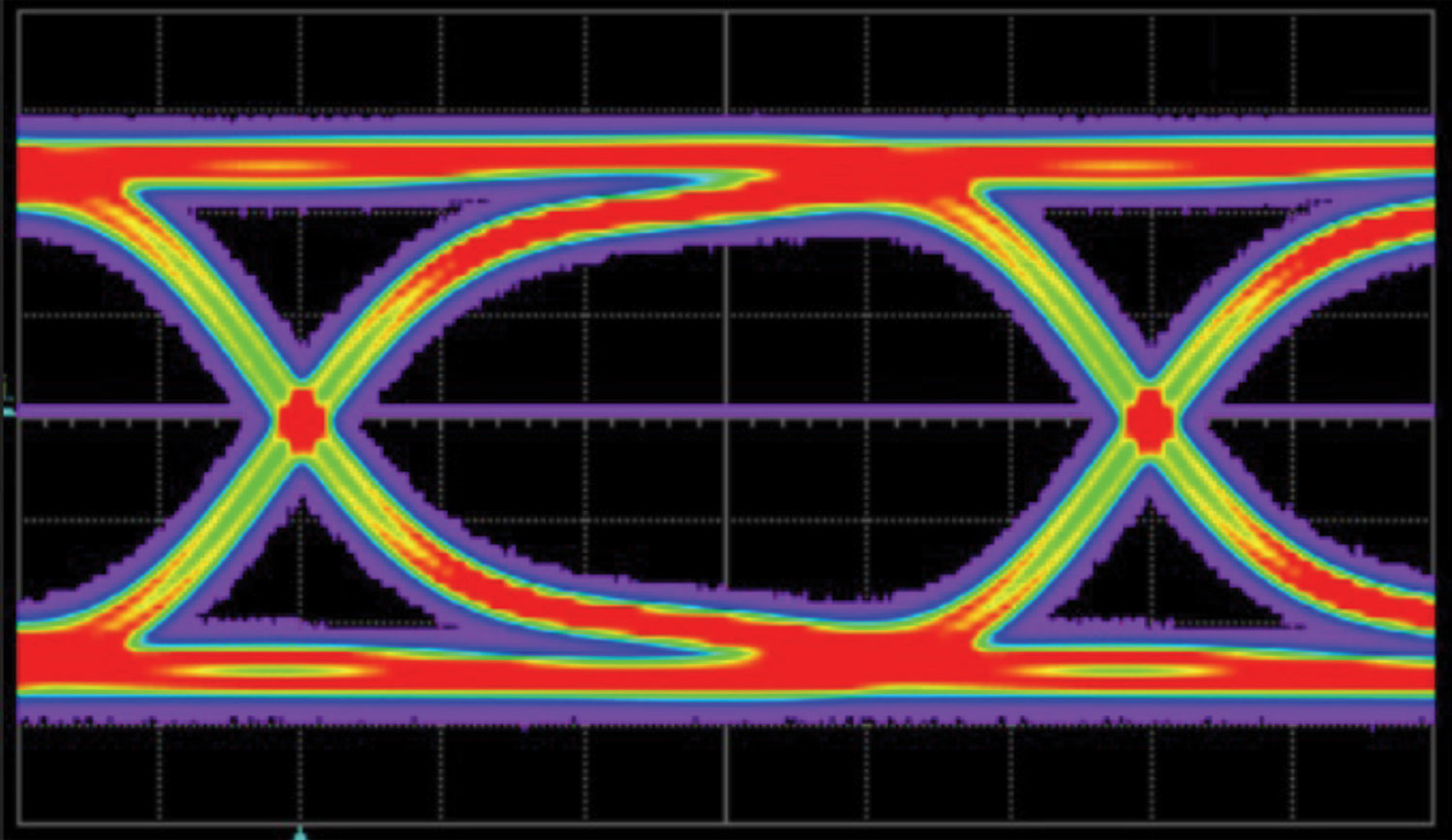
The eye diagram shown in Figure 4 is still an “ideal” diagram, as it consists of perfectly straight lines. An actual (real data) eye diagram looks more like the one shown in Figure 5 on page 50.
However, data signal voltage levels being below or above a predefined voltage threshold at the time of data transfer is an insufficient condition for reliable data transfer. It is also necessary to meet certain timing dependencies between data and synchronization signals.
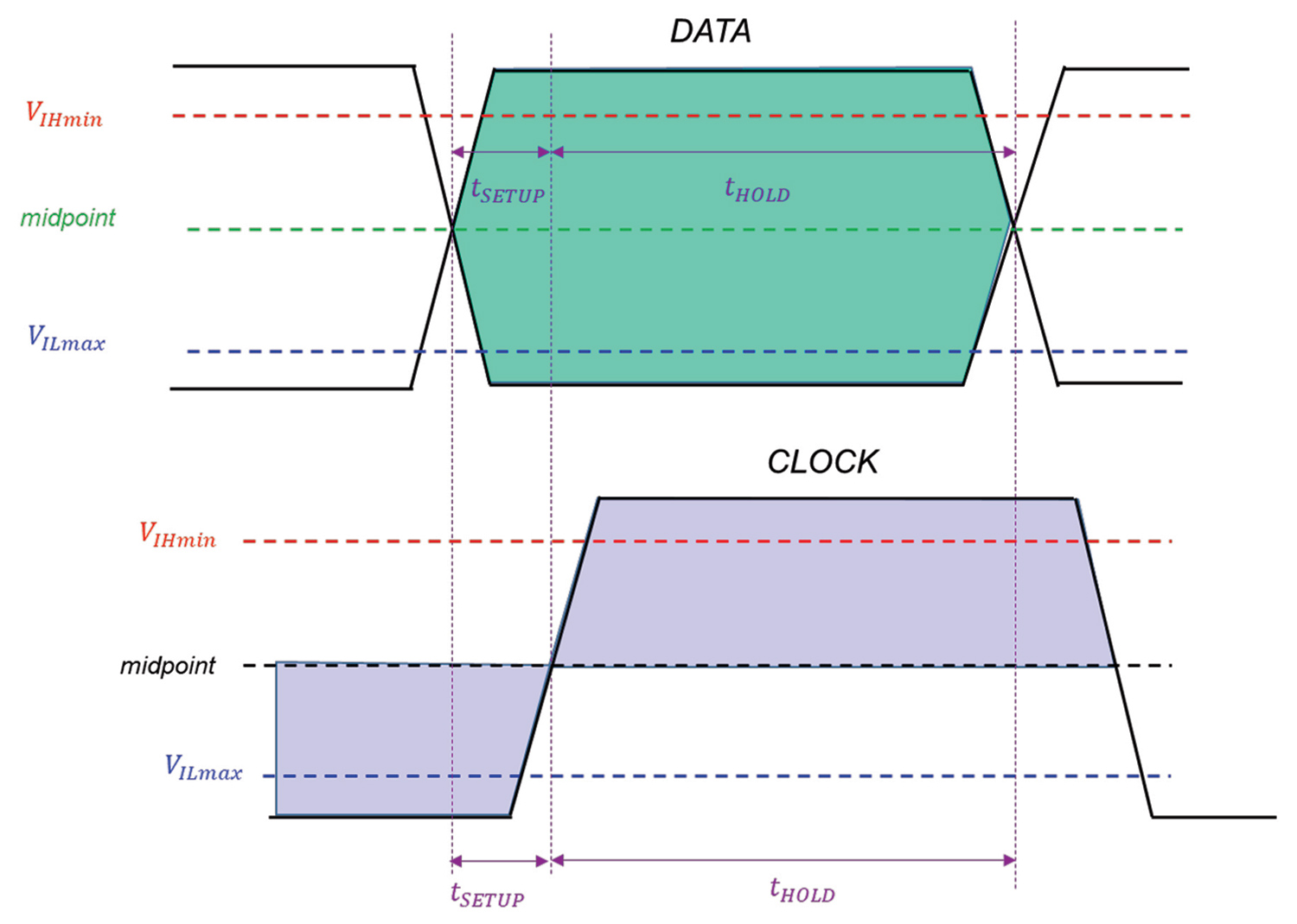
To explain those dependencies, let’s look at a specific case described in Figure 6 [3]. The synchronization signal, in this case, is the clock and the data is transferred (read) at the rising edge of the clock. We will assume that the clock and data signals are transitioning very quickly.
To guarantee that the proper data will be read, a valid data signal must be present for a certain time duration prior to the clock signal transition. This duration is referred to as a setup time (tSETUP). Additionally, it is also required that the data signal remains valid for a certain time duration after the transition of the clock signal. This duration is referred to as a hold time (tHOLD). Setup and hold times are properties of devices receiving the data and are often referred to as their timing requirements. If the timing requirements are not met, incorrect data can be read by the receiver.
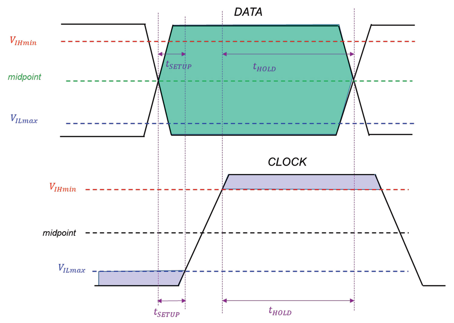
Using midpoint signal levels, the assumption of very fast signal transitions allows us to measure timing dependencies between the data and clock (setup and hold time). In other words, this assumption means we can neglect signal rise/fall time duration if those durations are much shorter than the duration when the data bit is valid. Suppose the clock period gets shorter, and we can no longer neglect signal rise/fall time duration. In that case, the evaluation of timing dependencies between the data and clock (setup and hold time) must account for slow signal transition. Figure 7 illustrates such a case.
The rising edge of the data is still very fast, but the clock transition is much slower. The duration of time between the clock transition from low and high level is now substantial compared to the duration of the data bit. During this long clock transition time the clock state can be either high or low, so we no longer can measure setup and hold time using midpoint levels. This case would require setup and hold time to be measured when the signals are crossing the low or high voltage threshold levels (VIL max, VIH min).
Evaluation and visualization of valid signal timing using the setup and hold time shown in Figure 6 is relatively easy, even with the clock and data jitter.
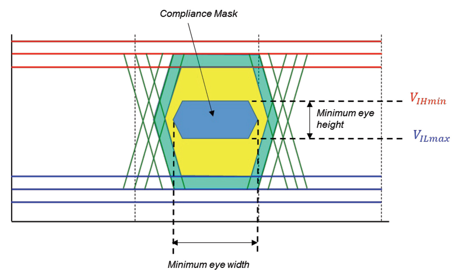
It is, however, quite difficult for the case shown in Figure 7 when taking jitter into account. That’s where the eye diagram can help.
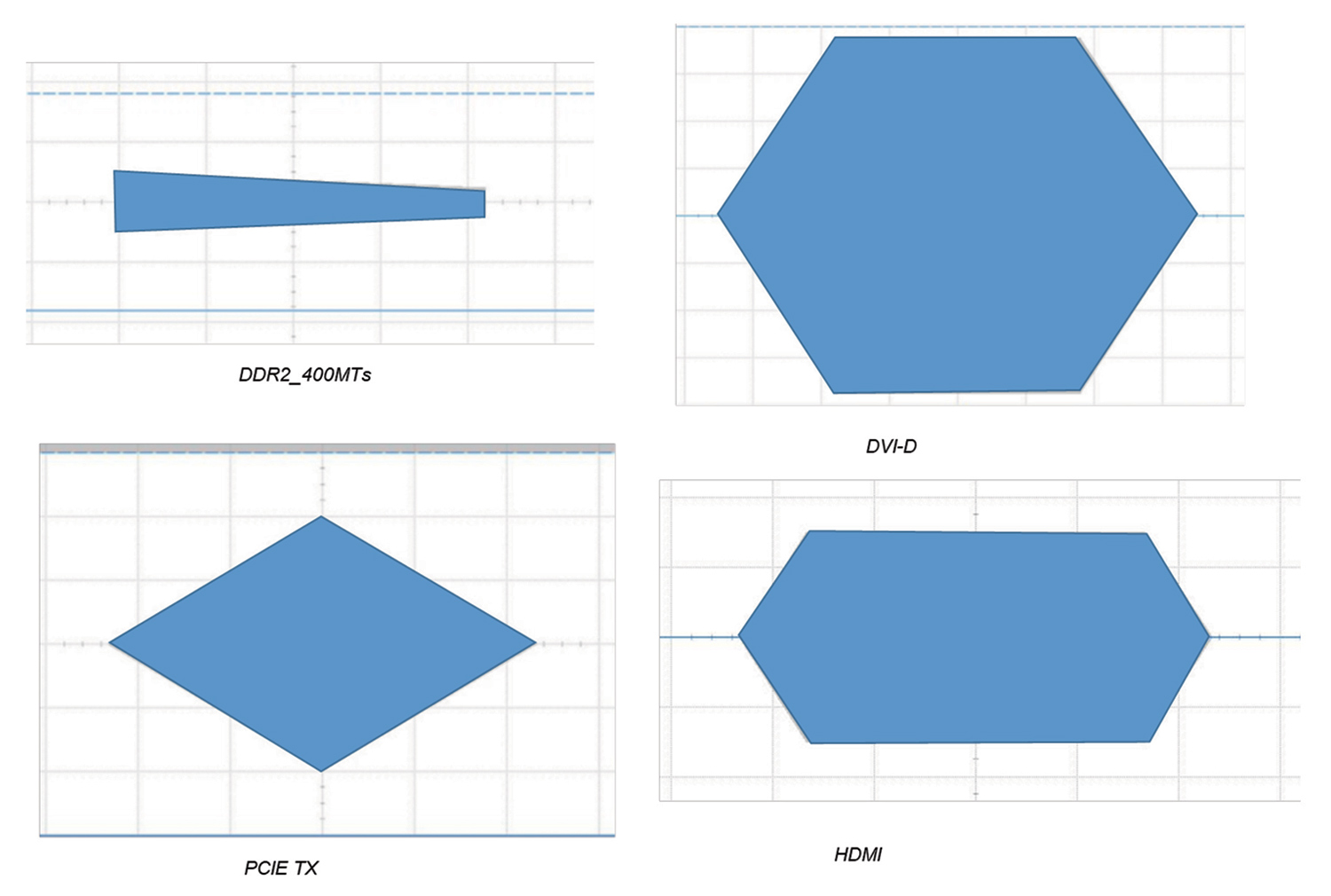
The data eye mask represents the “keep-out” region. Signals at the receiver must not cross the data eye mask region, or a violation of receiver timing requirements occurs. The mask is defined based on receiver properties and can have various shapes (rectangular, triangular, etc.). The data eye mask can be many different shapes, as shown in Figure 9.
- Herres, D., “The Eye Diagram: What is it and why is it used?” Test & Measurement Tips, August 2016.
https://www.testandmeasurementtips.com/basics-eye-diagrams - Behera, D., et al., “Eye Diagram Basics: Reading and Applying Eye Diagrams,” EDN, December 2011.
https://www.edn.com/eye-diagram-basics-reading-and-applying-eye-diagrams - Micron TN-48-09: LVTTL Derating for SDRAM Slew Rate Violations.
https://www.micron.com/support/-/media/e1b34fd94eb94b0bb9dce67694fe1046.ash


