Factors Involving ESD Protection Cell Design Selections
ow is the proper ESD Protection Cell chosen for a particular design application? Perhaps there is a more fundamental question—why is there more than one ESD Protection Cell in the first place? The answer to this second question will help answer the first.
An ESD Protection Cell must meet three basic criteria: it must be robust—able to carry required ESD current without being damaged; it must be effective—able to protect the rest of the Integrated Circuit (IC) during the ESD event, and it must be transparent—it must not interfere with normal IC operation. If the only two constraints were robustness and effectiveness, the ESD Protection Cell design would look like a perfect short— capable of carrying large amounts of current with no voltage build-up. Alternatively, if transparency were the only constraint, the ESD Protection Cell would look like a perfect open—drawing no current away from the rest of the IC circuitry. But both sets of constraints do exist, and the ESD Protection Cell Designer is faced with a requirement for perfectly contradicting attributes. The solution is to divide the operational space into multiple regions: a region where the ESD Protection Cell is robust and effective and a region where the ESD Protection Cell is transparent. How the operational space gets divided can have enormous consequences to the overall IC and ESD performance, and no one ESD Protection Cell can divide the space in a way that is applicable to every unique design application. The best ESD Protection Cell for a particular design application is the one that best divides the operational space between the transparency requirements and the robustness and effectiveness requirements.
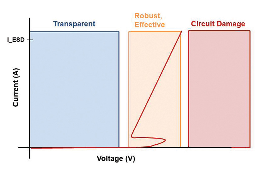
The simplest, and perhaps most common, example of a divided operational space is the splitting of the space into multiple voltage regions. As shown in Figure 1 (on page 18), the ESD Protection Cell draws significantly different amounts of current, depending on the applied voltage. Below a certain voltage level, the ESD Protection Cell draws almost no current and offers transparency to the rest of the IC circuit. This region is denoted in Figure 1 by the blue box on the left. Above a certain voltage, the ESD Protection Cell impedance lowers drastically, allowing current flow beyond the current delivered by the ESD event, without a voltage build-up that exceeds what is allowed by the rest of the IC circuitry—this is the region where the ESD Protection Cell is robust and effective and is denoted in Figure 1 by the orange box. If the voltage extends beyond the orange box, the ESD Protection Cell is not effective because it can no longer protect the IC. The region in the orange box is commonly referred to as the ESD Design Window. Space was purposefully left between the regions in Figure 1 — this space represents design margin.
If the operational space is not well-understood and not divided correctly, unexpected problems may arise. Take, for example, a fault condition which takes the pad voltage beyond the normal operating voltage. If this condition is not anticipated in the division of the voltage regions, the voltage could exceed the transparent region and initiate the ESD Protection Cell’s low impedance state. This could interrupt the IC operation or even cause damage to the IC or the ESD Protection Cell. This effect also leads to what is known as Electrical Overstress (EOS) damage [See Ref. 3].
As technologies shrink, the voltage level at which circuit damage occurs is reducing faster than the transparency requirements reduce, leading to a tightening of the window in which the ESD Protection Cell can operate in its low impedance state [1]; this narrow window is also very common in high voltage (e.g., >20V) design applications [2], where lower margin may be present between allowed operating conditions and on-set of circuit damage. Due to the narrowing of this window, it becomes more and more difficult to keep the ESD Protection Cell’s low impedance state fully in the ESD Design Window, and other techniques are applied.
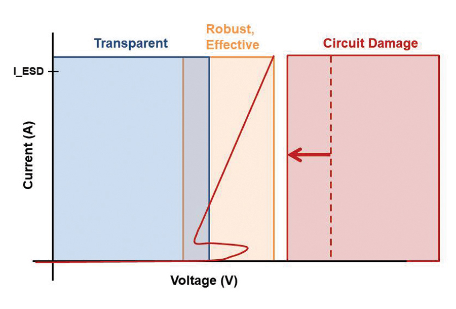
One potential solution to the tightening ESD Design Window is to allow the ESD Design Window to start encroaching onto the Transparent Region, as shown in Figure 2.
In this scenario, as the region where the IC circuit is damaged pushes to the left, the ESD Design Window is also pushed to the left and starts to overlap the region where the ESD Protection Cell must be transparent. To continue simultaneously meeting all the requirements, it must be ensured that the ESD Protection Cell’s trigger voltage (the voltage at which the ESD Protection Cell switches from its high-impedance state to its low-impedance state) remains outside the Transparent Region. It must also be ensured that, even if the ESD Protection Cell does enter the low-impedance state, it cannot remain in this state. In Figure 1, this was ensured because the entire low-impedance portion of the ESD Protection Cell’s i-v curve was outside the Transparent Region. Now that a portion of the i-v curve extends into the Transparent Region, the conditions under which the ESD Protection Cell remains in the low-impedance state must be well understood and compared to the normal operating conditions, so that it is certain that the ESD Protection Cell will not remain in this state if it is triggered.
There is an important distinction that must be made—it is the actual application that matters, not the intended or assumed application. Take, for example, an IC input pin versus an IC power supply pin. The first instinct may be to deem the power supply pin as riskier than the input pin, due to the fact that the power supply pin will likely see an applied voltage capable of supplying significant current—current which could allow the ESD Protection Cell to remain in its low-impedance state. Similarly, the input pin may be viewed as safer because it will likely be driven by a signal with limited current: current that cannot maintain the low-impedance state. But how is this input pin going to be applied in the actual system? What if the input pin is used to set a permanent state, and will be tied directly to a power supply in the system? In this scenario, the input pin is no less risky than the power-supply pin. It is crucial that the system designer knows the limitations of the IC and that the IC designer knows how the IC will be used in the system.
Thus far, the examples of dividing the operating space into regions have centered on voltage. But what about other characteristics that differentiate the normal operating signal characteristics from the ESD event characteristics? One such characteristic is rise-time—how quickly the signal moves from low to high voltage. Under ESD events, very fast rise-times are present, and, if the normal operating signals are slower, then ESD Protection Cells can be equipped with triggering circuits that respond differently to ESD events than to normal operation signals.
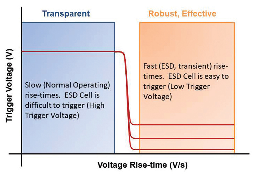
Figure 3 shows an example of such a characteristic. In this example, the regions are separated, not by voltage, but rather by the voltage rise-time. For the purpose of illustration, consider the two regions of Figure 3: 1) Slow rise times on the left and 2) Fast rise times on the right. With this dual strategy, the trigger circuit is designed to more easily trigger for faster rise-times than slower ones— thus, the ESD cell can be tuned to be difficult to trigger during normal operation, but easy to trigger under ESD events. Figure 3 shows three different ESD Protection Cell curves– this is to emphasize that not only can the ESD Cell be designed to have different trigger voltages for slow and fast rise-times, but that the difference in the trigger voltage can also be controlled, depending on the specific characteristics of the ESD Protection Cell. If the separation of the rise-time regions is not made correctly, or transient events are present that were not anticipated by the ESD Protection Cell designer, then triggering can occur at unintended times. One such example occurs in ‘hot-plugging’ applications: scenarios where the system has to be connected to power systems that are already energized. These types of events produce voltage rise-times that are difficult to quantify and make it difficult to properly determine the needed selectivity of the trigger circuit.
Another difference between normal signals and ESD events that can be leveraged by the ESD Protection Cell designer is the environment in which the IC is present. Many ESD Protection requirements are intended for safe-handling before the IC is placed in the actual system. If the ESD Protection Cell can detect if it is in a system, it can be designed to respond accordingly. For example, the presence of power to the IC can be used as a criterion for confirming the IC is in an active system. In this scenario, an ESD Protection Cell could be equipped with a triggering circuit that is disabled when power was supplied to the IC. While this strategy can be used to successfully protect the IC during handling, it limits the effectiveness of the ESD Protection Cell during normal operation. If system-level ESD performance is depending on the IC’s internal ESD Protection Cells for part or all of the ESD performance, then this needs to be known to the IC designer so that proper ESD Protection Cell selection can be made.
While most of this article has focused on ensuring that the ESD Protection Cell’s operation properly selects between ESD events and normal operating signals, there are other factors that must be considered in the ESD Protection Cell selection process. One such factor is area—the IC must be able to accommodate the area consumed by the ESD Protection Cell. Similarly, there may be processing options required for the ESD Protection Cell that are not required for the rest of the IC design. Adding these options may increase the cost of the IC fabrication process, and a different ESD Protection Cell may be a less expensive alternative, even it consumes more area. Another factor is the total capacitive loading—some applications limit the amount of capacitance, further limiting the overall size and type of devices used in the ESD Protection Cell.
Additional constraints can come from the required behaviors of the system outside normal operation. As an example, a common requirement is ‘fail-safe’ ESD design; in this scenario, the ESD Protection Cell has to be designed to ensure that the signal pin does not offer a low-impedance path to a power supply when power to the IC is lost or purposefully removed. In many ESD Protection strategies, a forward-biased diode is used to a positive supply rail. In these scenarios, loss of power would violate the fail-safe requirement, leading to a conflict between the ESD Protection Cell and the Transparency requirements.
While the above design spaces apply to digital and analog applications, the applications for RF designs often allow less separation of the “ESD Design Space” from the “RF Design Space.” This is due to overlap in the spectral content of the two spaces and to the sensitivity of the RF circuit to parasitics. For this reason, a co-design strategy is more desirable—that is, the ESD Design Space is shared with the RF Design Space in such that the ESD Cell becomes part of the RF functionality.
The ESD Protection Cell Designer is faced with the challenge of simultaneously meeting numerous constraints—many of which require conflicting attributes. An ESD Protection Cell must present a high-impedance to normal operating signals and yet a low-impedance to ESD events. Meeting both requirements simultaneously is achieved by dividing the operation space between normal operation signals and ESD events and designing an ESD Protection Cell that behaves very differently in the different regions. Due to the myriad of normal operating signals, there is no ‘one-size-fits-all’ ESD Protection Cell and selecting the proper ESD Protection Cell requires careful consideration of the ESD Protection Cell’s behavior across the entire operational space.
- G. Boselli, J. Rodriguez, C. Duvvury, and J. Smith, “Analysis of ESD protection components in 65nm CMOS technology: Scaling perspective and impact on ESD design window,” 2005 Electrical Overstress/Electrostatic Discharge Symposium, Tucson, AZ, 2005, pp. 1-10.
- B. Keppens, M. P. J. Mergens, C. S. Trinh, C. C. Russ, B. Van Camp, and K. G. Verhaege, “ESD protection solutions for high voltage technologies,” 2004 Electrical Overstress/Electrostatic Discharge Symposium, Grapevine, TX, 2004, pp. 1-10, DOI: 10.1109/EOSESD.2004.5272593.
- Charvaka Duvvury, Alan Righter, Hans Kunz. “Impact from IC On-Chip Protection Design on EOS.” In Compliance Magazine, July 2020.


