EMC concepts explained
PCB Return-Current Distribution in the Stripline Configurations
L

ast month’s article, [1], discussed the distribution of a PCB return current in a microstrip configuration. This article discusses the current distribution for the stripline configurations.

Return Current Distribution in a Symmetric Stripline Configuration
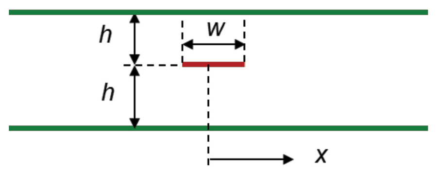
Consider a symmetric stripline configuration, shown in Figure 1, where a PCB trace of width w is placed in-between two planes, at the same distance h from each plane; x is the distance from the center of the trace.

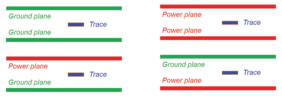
The possible plane combinations are shown in Figure 2.

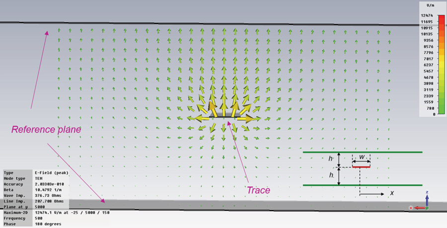
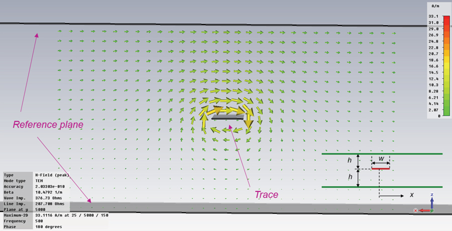
Figure 3 and Figure 4 (on page 14) show the CST Studio simulations of the E and H fields, respectively [2].
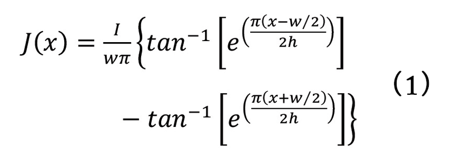
The current distribution on each reference plane is described by its current density [3] J(x):
equation
Example of a Symmetric stripline configuration
Figure 1: Symmetric stripline configuration
The current distribution on each reference plane is described by its current density [3] J(x):
equation
Example of a Symmetric stripline configuration
Figure 1: Symmetric stripline configuration
Eq. (1) represents the current density in just one of the two reference planes. The total reference plane current density is twice of that in Eq. (1).

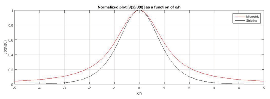
Figure 5 shows the Matlab plot of (normalized) current density as a function of x/h for both the symmetric stripline and a microstrip configuration.

Example of Plane combinations for a symmetric stripline
Figure 2: Plane combinations for a symmetric stripline
Note that the stripline current does not spread out as far as in the case of a microstrip line. At a distance ±4x/h from the center, the current density in a stripline rapidly decays toward zero, while in a microstrip, there’s still a noticeable non‑zero current density.

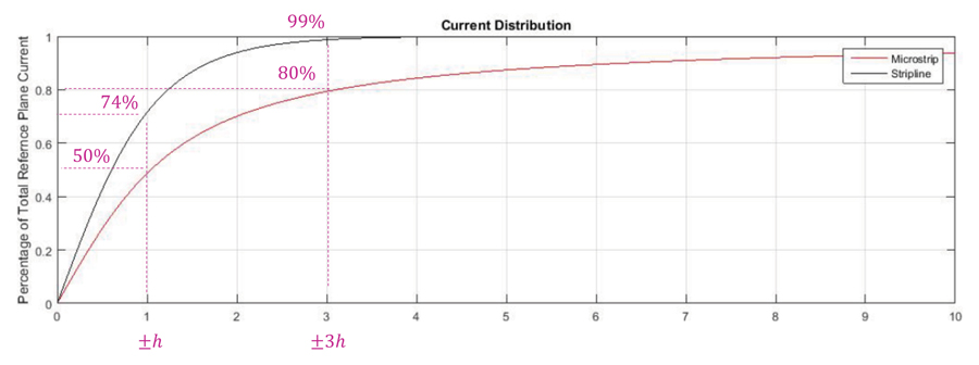
Figure 6 shows the % of the total return current for both configurations, contained in the portion of the plane between ±x/h of the centerline of the trace.

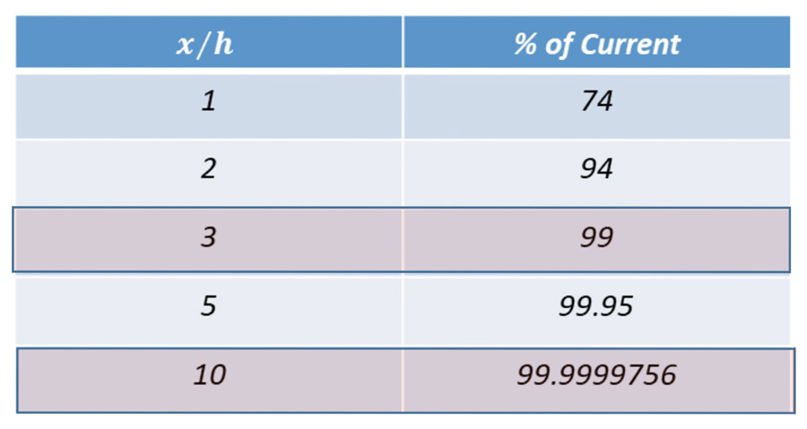
Table 1 shows more detailed results for the stripline configuration [3].

In the stripline configuration, 99% of the current is contained within ±3 x/h. Virtually all current is contained within ±10 x/h.

Example of Symmetric stripline - simulated E field
Figure 3: Symmetric stripline – simulated E a field
Example of Symmetric stripline -simulated H field
Figure 4: Symmetric stripline -simulated H field
Return Current Distribution in an Asymmetric Stripline Configuration
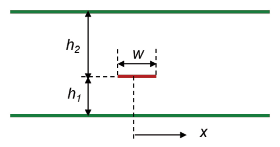
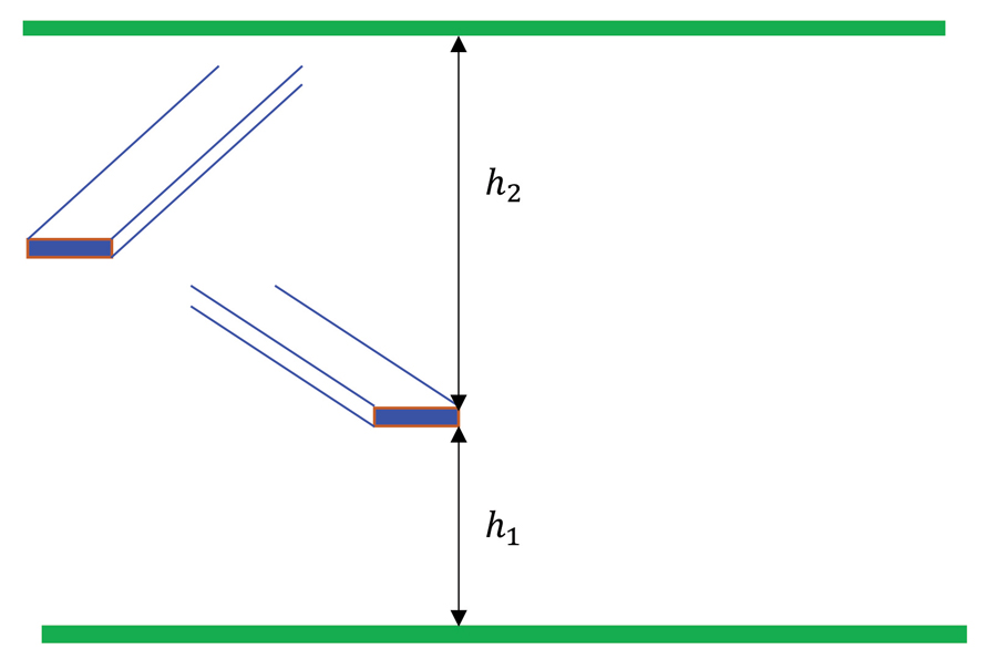
Consider an asymmetric stripline configuration, shown in Figure 7, where h1 is the distance between the trace and the closest plane, where h2 is the distance between the trace and the furthest plane.

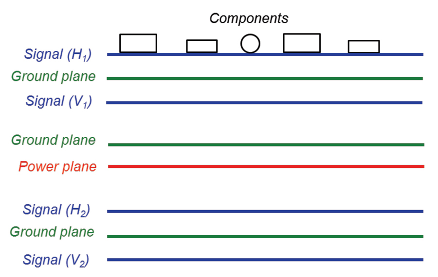
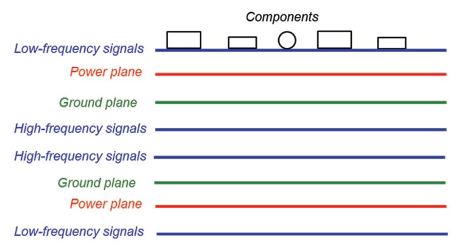
Figure 8 shows an 8-layer PCB where the signal V1 is placed between two ground planes, while the signal H2 is routed between a power plane and a ground plane.

Graph of Current density in a symmetric stripline (Matlab)
Figure 5: Current density in a symmetric stripline (Matlab)
Graph of Cumulative distribution of the return current
Figure 6: Cumulative distribution of the return current
Table of Cumulative current in % for a stripline configuration
Table 1: Cumulative current in % for a stripline configuration
Figure 9 shows an asymmetric stripline configuration where two orthogonally routed signal layers are placed between the reference planes.

Figure 10 shows a PCB topology where two high-frequency traces are placed between the reference planes.

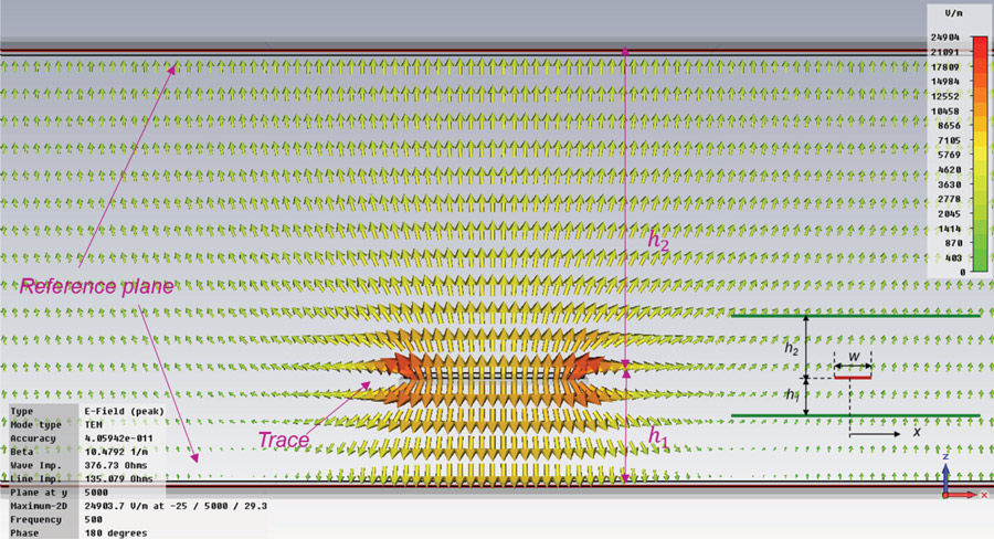
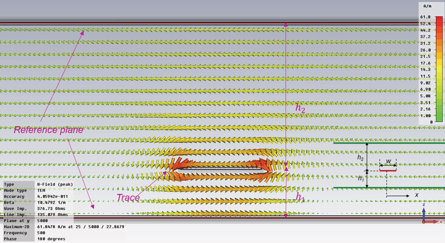
Figures 11 and 12 on page 16 show the CST Studio simulations of the E and H fields, respectively.

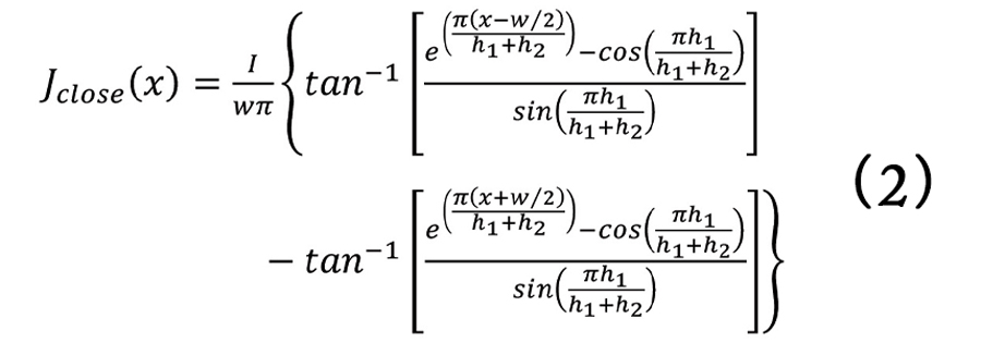
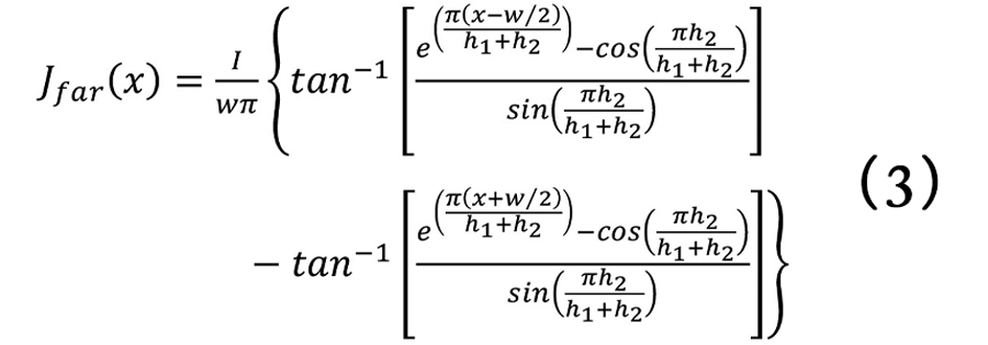
The current distribution for the close and far reference plane is described by its current density [3] J(x) as

equation
equation
Example of Asymmetric stripline configuration
Figure 7: Asymmetric stripline configuration
Example of an 8-layer board PCB with a single trace between two planes
Figure 8: 8-layer board PCB with a single trace between two planes
Example of an Asymmetric stripline configuration
Figure 9: Asymmetric stripline configuration
Example of an 8-layer board PCB with two traces between the reference planes
Figure 10: 8-layer board PCB with two traces between the reference planes
Figure 13 shows the Matlab plot of (normalized) current density as a function of x/h for both planes.

Note that, directly under the trace, 75% of the current flows on the closest plane and 25% on the far plane. At distance, greater than ±3 x/h, the currents in both planes are of the same magnitudes.

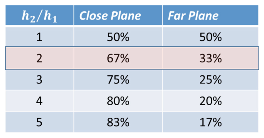
Finally, Table 2 shows the percentages of the return current in each plane for different h2/h1 ratios [3].

Example of an Asymmetric stripline - simulated E field
Figure 11: Asymmetric stripline – simulated E field
Example of an Asymmetric stripline -simulated H field
Figure 12: Asymmetric stripline -simulated H field
Graph of the Current density in an symmetric stripline
Figure 13: Current density in an symmetric stripline (h2 = 3h1)
References
  1. Bogdan Adamczyk, “PCB Return-Current Distribution in a Microstrip Line,” In Compliance Magazine, November 2020.
  2. Scott Piper, CST Microwave Studio Simulations, Gentex Corporation, 2012.
  3. Henry W. Ott, Electromagnetic Compatibility Engineering, Wiley, 2009.

Table of Percentages of the return currents for different h2/h1 ratios
Table 2: Percentages of the return currents for different h2/h1 ratios
Table of Percentages of the return currents for different h2/h1 ratios
Table 2: Percentages of the return currents for different h2/h1 ratios
References
  1. Bogdan Adamczyk, “PCB Return-Current Distribution in a Microstrip Line,” In Compliance Magazine, November 2020.
  2. Scott Piper, CST Microwave Studio Simulations, Gentex Corporation, 2012.
  3. Henry W. Ott, Electromagnetic Compatibility Engineering, Wiley, 2009.
Share this story:
Dr. Bogdan Adamczyk headshot
Dr. Bogdan Adamczyk is professor and director of the EMC Center at Grand Valley State University (http://www.gvsu.edu/emccenter) where he regularly teaches EMC certificate courses for industry. He is an iNARTE certified EMC Master Design Engineer. Prof. Adamczyk is the author of the textbook “Foundations of Electromagnetic Compatibility with Practical Applications” (Wiley, 2017) and the upcoming textbook “Principles of Electromagnetic Compatibility with Laboratory Exercises” (Wiley 2022). He can be reached at adamczyb@gvsu.edu.