s electronic systems become more pervasive in today’s world, particularly in mission critical systems, it becomes more imperative that they do not fail within the warranty period. Electrical overstress (EOS) and electrostatic discharge (ESD) damage are two of the major reasons for field failures. Designers of these electronic systems must be aware of the various methods by which EOS and ESD damage can occur and thus apply multiscale, multidomain, and multiphysics simulation solutions to address these issues.
The performance, reliability, and longevity of an electronic system that has direct exposure to system ESD events depend on the system’s immunity from an ESD discharge event. Yet, the components of the system are designed independently with predefined specs and margins in mind. Because the components come from various sources, and often from different companies, they are usually designed by separate teams working in silos and in accordance with predefined margins. As a result, the ESD consequences at the system level can be difficult to identify and mitigate.
What’s more, ESD is not a single physics problem; it’s a combined electrical, thermal, and mechanical problem. Electromagnetic (EM) fields can become second- and third-order effects for other devices within the system, and the mitigation challenge stretches from design into test and measurement. The ability to deliver high performance, integrated systems that meet customer demand while reducing design costs requires a highly accurate and efficient process for simulating across a cohesive chip, package, and system environment.
Therefore, system-level ESD failure is a growing concern in electronics design and is a cumulative sum of errors of ESD failure and interaction between integrated circuit(IC), components, package, printed circuit board (PCB), and system. (See, for example, Reference [1] where the principles of system-level co-design have been described for both mobile and automotive applications.)
The modeling and simulation methodology for system-level ESD testing in compliance with IEC61000-4-2 [2] is outlined in Figure 1. As stated in Reference [3], realistic models of an ESD gun generator, connector, ESD protection element, PCB plane, trace /vias, and IC ESD are needed in the simulation. This article also briefly addresses modeling technology and a list of solver technology as well.
In particular, the article notes that a realistic chip ESD model is important for the determination of voltage/current on the chip pins. Other recent works [4,5,6] focused on the correctness of the ESD gun pulse, protection elements and models for PCB traces, and correlation versus measurements. However, the difficulty in creating a full-wave compliant model for various forms of connectors present a challenge in system-level ESD simulation. In this article, we outline a comprehensive chip-package-system ESD simulation methodology that addresses the interface modeling between the ESD gun and system and the interface modeling between the system and IC chip(s).
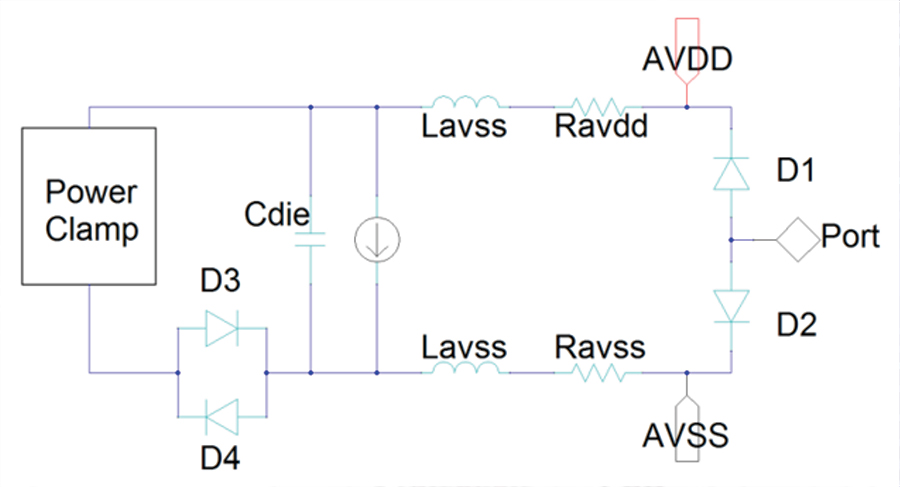
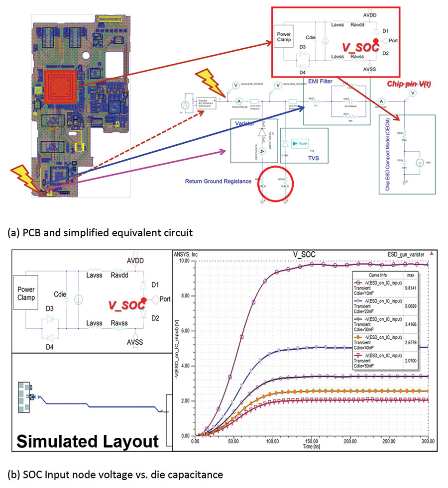
The first aspect that we will focus on is accurate device and component modeling at the chip level. A chip ESD compact model (CECM) (Figure 2) is an accurate and compact representation of a die. It contains a compact passive model capturing on-die parasitics, the current signature model of ports for a specific scenario [7], and optional ESD protection elements (e.g., diodes and RC-based clamps). In the passive model, the total capacitance (i.e., Cdie) of a power/ground domain pair includes power/ground coupled capacitance, on-chip decoupling capacitance, and capacitors from non-switching cells and their C-loads. Because the ESD spectrum is broadband, the die model must be accurate in the GHz range. Therefore, a reduced RC or RLC network model of the die is included.
CECM is a SPICE model that enables users to perform various “what if” analysis, such as leaving the on-chip ESD protection in or out to see how the PCB ESD protection performs in PCB ESD simulation. Without on-chip ESD protection elements in CECM, the V(t) and I(t) on the chip pin (or pad) becomes the energy that is propagated through the connector/PCB/on-board ESD protection elements. In general, the larger the on-chip capacitance (Cdie), the smaller the amplitude of voltage/current at the chip pins. Since this is a power-on PCB ESD simulation, the voltage and/or current amplitude should not have excessive value at the chip pins. When running a PCB ESD simulation with chip ESD protection elements in CECM, the V(t) and I(t) of the chip pins will be reduced accordingly, thereby minimizing over design while helping to ensure that overall ESD protection is adequate.
A key part of this holistic approach starts at the chip level with an ESD simulation tool that enables design teams to plan, verify, and signoff intellectual property (IP) and full-chip system-on-chip (SoC) designs for integrity and robustness to combat ESD[8,9]. ESD analysis is performed using such a tool at the layout and circuit levels to help users identify and isolate design issues that can cause chip or IP failure from charged-device model (CDM), human body model (HBM), or other ESD events once the design is verified.
The starting point is the chip ESD compact model(CECM), which is a synthesized model in a SPICE netlist format that can be used in any SPICE simulation or system-level tools. This behavioral model mimics the behavior of the chip power-delivery network along with the ESD protection devices embedded in it. A chip power model (CPM) can be used by system vendors who require a highly accurate abstracted model of the chip power delivery network to perform system-level power-integrity analysis and optimization. Think of it as reducing a massive billion-node+ on-chip power grid to a compact spice model that can be used for package or system simulations.
In the process, the integrity of the model is maintained in both the time and frequency domains. The model does not preserve any actual design information and hence protects designers’ IP from being shared with a third-party vendor performing system assembly. Systems engineers can use any number of CECMs as part of their system-level ESD analysis. This enables virtual prototyping at the system level. The system vendor can request the integrated circuit (IC) vendor’s respective models and can create a virtual prototype for the complete system to do a trade-off analysis.
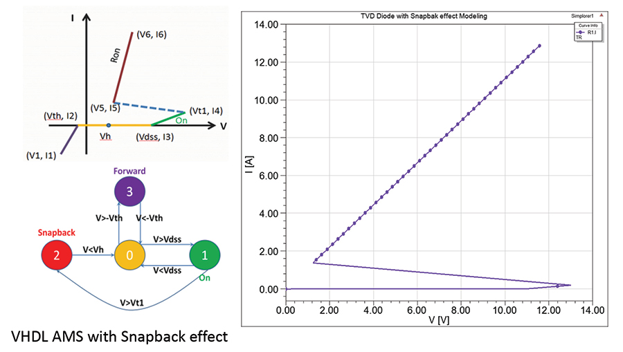
Commercial transient voltage suppressor (TVS) diode vendors provide model parameters in their data sheets. Commercial simulation software can provide an approximate model for the TVS diodes that is dependent on input parameters from the datasheet. Figure 3 shows how software can support TVS snapback effect modeling with very high-speed integrated circuit hardware description language – analog mixed signal (VHDL-AMS). VHDL-AMS is a standardized language used for describing digital, analog, and mixed-signal systems.
An ESD filter can be modeled in a full-wave 3D finite element method (FEM) solver using a circuit tool. This full-wave 3D FEM model is parameterized with manufacturing tolerance. This model can be directly plugged into the circuit simulation tool as an EM-based parametric model component and verified with measured result. A high-frequency structure simulator (HFSS) provides fully encrypted component designs for electronics device/modules and systems that protect customer IP.
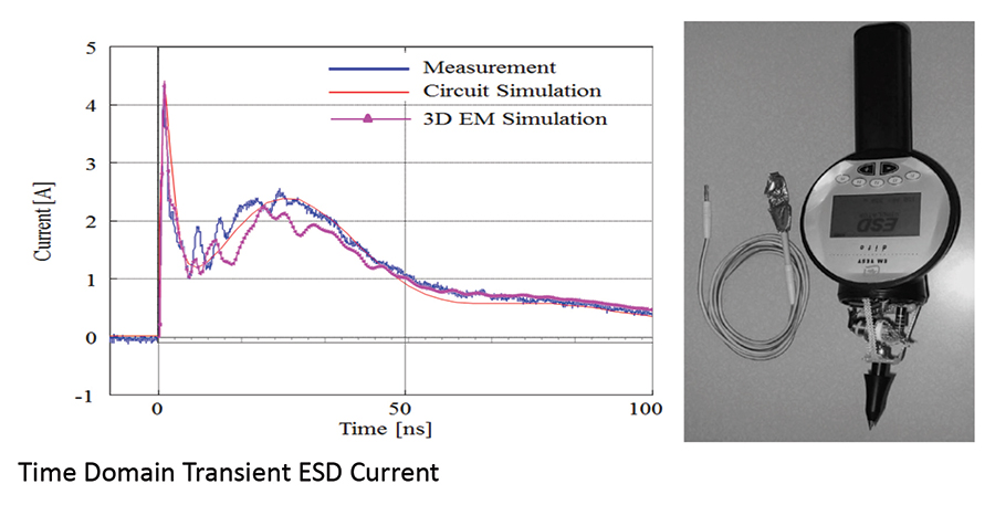
ESD generators are used for testing the robustness of electronics subjected to ESD events. There are two different discharge methods for an ESD simulator, and this article replicates a contact type ESD gun model [8,10], as shown in Figure 4 on page 34 and with good correlation of measurement result. HFSS can handle a full transient solution to make a complete ESD gun model with transient behavior. This FEM based transient simulation models ESD gun radiation effects as well as the cable interconnect network according to standard, IEC 61000-4-2.
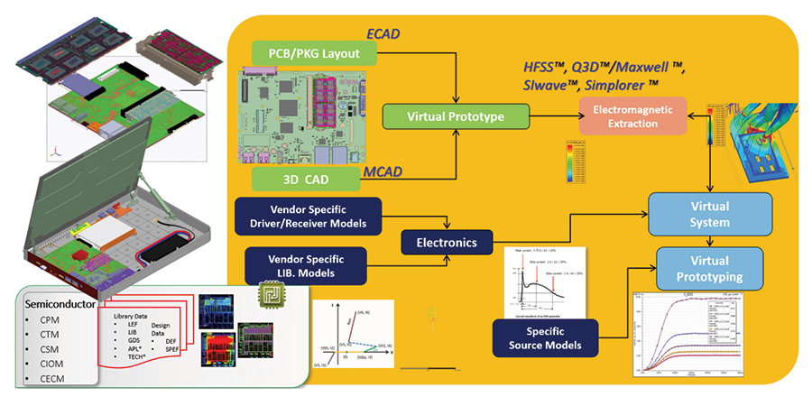
Finally, a workflow is needed to incorporate all the different elements of the system previously discussed. Models of chip, discrete components, ESD zapping, and package and board can be plugged into the workflow to enable a system level chip-package-board and chassis solution for ESD simulation, as shown in Figure 5.
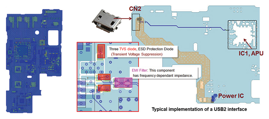
Efficient ESD design for the system must recognize energy entering the interface IC pin in terms of a residual pulse [10]. Typical implementation of a USB2 interface is shown in Figure 6 as a first application example [10]. System-level ESD protection is primarily ensured with an external TVS, CMF/EMI filter, and/or ESD filter.
As secondary protection, IC pins have their own respective on-chip ESD protection that meets both human body model (HBM) and charged device model (CDM) requirements. The IC1 in the PCB schematic in Figure 6 shows differential pins for the USB that need protection using a TVS device. As will be discussed here, the common mode filter (CMF) plays an important role in overall protection efficiency. CMF is primarily intended to filter common mode noise that results from two phase lags between the differential signals (either unequal PCB trace lengths or unequal loadings) or from EMI pick-up through a USB cable. All of these protection devices have parasitic capacitance that will affect high-speed signal distortion. The optimum placement of components in Figure 6 determines the effectiveness of ESD protection while having minimum impact on signal integrity.
Figure 6 also shows the actual board implementations for ESD protection with the processor IC, the TVS diode, and EMC filter or CMF, board traces, and the micro USB receptacle on the left. Most of the USB signals are routed within inner layers in a strip-line configuration to minimize crosstalk between the traces and coupling from radiation sources such as RF chips and/or the ESD gun. The EMI filter is placed after the TVS, precisely between the TVS and processor IC. The TVS is placed just behind the receptacle. The PCB interconnect from the TVS to the processor IC is about 5.5 cm long.
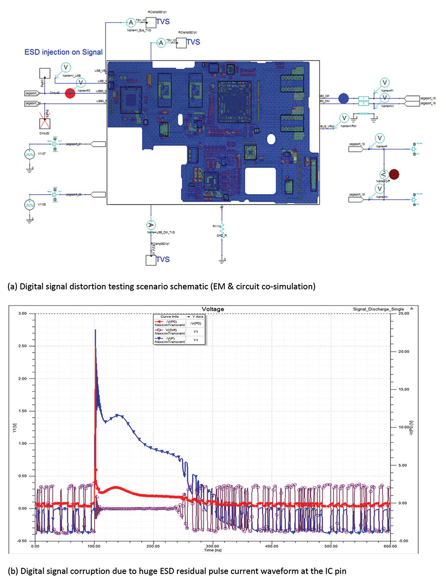
Chip-package-system (CPS) transient simulations are performed as shown in Figure 7 on pages 36 and 37 to determine the residual pulse current waveform at the IC pin while high speed USB communication is happening between AP and USB device. The simulation considers the TVS, the PCB interconnects, the passive devices, and the CECM.
We injected the 5kV ESD discharge current waveform (red curve) on the USB connector shield location (120Vp @ USB connector ground) and detected a residual voltage pulse on the processor IC input signal trace, 2.78Vp (blue curve). Figure 7 (b) shows specific failure mechanisms activate during an ESD event, depending upon the nature and magnitude of the event and the circuit elements (device level) encountered by the over stressed pulse. Semiconductor junction leakage may occur, or dielectric breakdown or latch-up could be triggered. Each of these conditions can lead to thermal issues, melting or cracking, and shorting or open circuits, which in turn may cause additional failures.
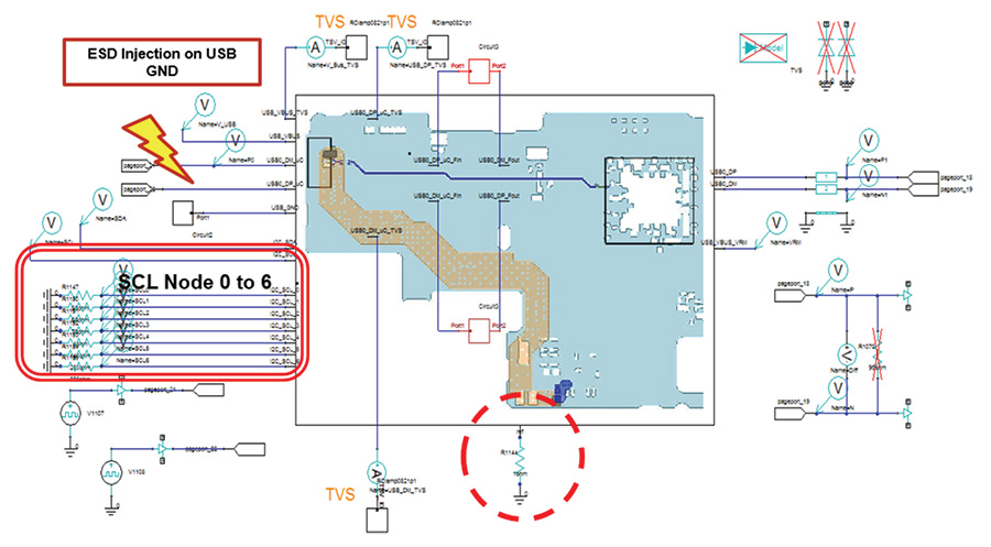
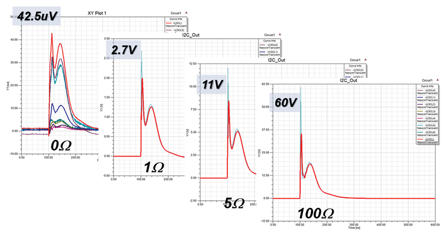
Another example demonstrates ESD propagation modeling [10] with a return ground path effect as shown in Figure 8 on page 37. This return path impacts ESD propagation on PWR, GND and signals. In this model, we intentionally selected the SLC line on the mobile PCB to see how the return ground path effect would depend on the impedance variation in the range of zero to hundreds of ohms.
With zero-ohm reference return current path, we get 42.5uV on SLC node1. With one ohm return ground path impedance, we get 2.7V on SLC node1, which is large enough to create ESD damage on the SMD. Figure 9 on page 38 shows the waveform on the highlighted objects.
A what-if analysis was done on the design to simulate the system with different chip models capturing different Cdie. Figure 10 on page 38 shows chip pin voltage V(t) changes with different chip Cdie in CECM(s).
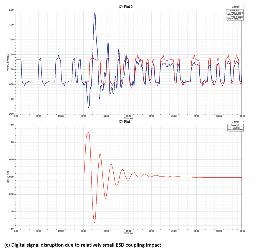
In another simulation example, we analyzed a USB2 interface’s impact on an ESD event and provided a system design guide in terms of ESD propagation. System-level ESD protection can be ensured by different module levels, and, at the IC level, IC pins have their own on-chip ESD protection. This, however, does not necessarily mitigate transient effects within the system. The USB2 connector shield was stressed with the ESD discharge current from the 5kV ESD gun model, and the engineers were then able to simulate the transient effects. This type of methodology easily allows teams to make additional design trade-offs in terms of device spacing and additional filtering and protection mechanisms.
In the third example, we analyzed the ESD current propagation with a return ground path effect, which can impact power, ground, and signals. There are challenges in measuring voltage or currents on IC pin or package bump location, and it is impossible to probe them without breaking the IC package. When designers use software to do virtual prototyping for system-level ESD, there are no such measurement limitations. Without this barrier, designers can get insights on whether to put more ESD protection on PCBs or on-chip.
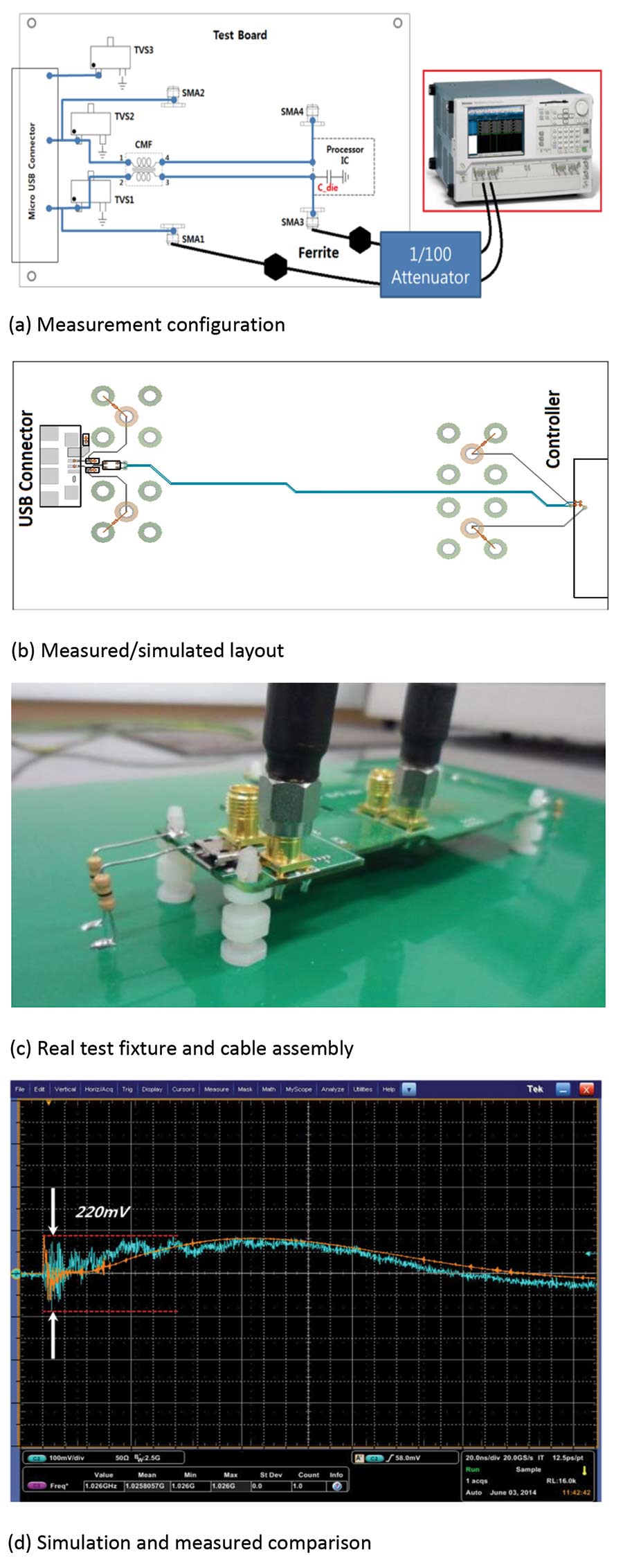
Finally, we must validate this simulation approach with test and measurement as part of the validation process. The ESD discharge current waveform injected by the ESD generator and the voltage waveform on the processor IC input signal trace are measured to validate the simulation results, as shown in Figure 11(a) on page 39. The injected current waveform is measured using a test board and a current probe shown in Figure 11(b).
The voltage waveforms across the TVS and CMF are measured using a custom designed test board with three TVS diodes and a mounted CMF, as shown in Figure 11(c). To measure the voltage waveform, two 50-ohm coaxial cables were used to connect the test board (via SMA connection) to the oscilloscope with an attenuator and ferrite beads.
Figure 11(d) shows the measured (sky blue) and simulated (orange) voltage waveform on the USB connector pin and processor IC input signal trace. This allows us to verify the accuracy of simulation results as shown at probe point at SOC input pin.
IC and systems design can no longer be viewed as separate disciplines when it comes to analyzing and preventing ESD. The complexity of SoCs, the boards they sit on, and the packages within which they are located are all connected and can be potentially affected by ESD in isolated areas[10].
Now, there is a comprehensive chip-package-system (CPS) ESD simulation methodology that addresses IEC61000-4-2 testing conditions. It starts with an innovative full-chip ESD compact model, which is then combined with full-wave transient models of the ESD gun, ESD protection devices, PCBs with vias, advanced packaging (including 3D ICs), and connectors — for unrivaled system-level ESD analysis.
It can be challenging to protect against ESD in complex, high-speed technologies, as these require careful signal path design and must survive system-level ESD requirements. Simulation, therefore, has become an essential part of designing ESD robust electronic systems. A holistic methodology effectively and efficiently locates and mitigates ESD risks well before hardware prototypes are available, saving teams time, effort, and money. This approach can lead to more reliable and efficient systems in crucial applications, such as automotive, avionics, 5G and, yes, in-flight entertainment systems.
- C. Duvvury and H. Gossner, System Level ESD Co-Design, John Wiley & Sons, 2015.
- IEC61000-4-2, “Electromagnetic Compatibility (EMC) – Part 4-2: Testing and Measurement Techniques – Electrostatic Discharge Immunity Test,” Ed. 2.0, 2008-12.
- L. Lou, C. Duvvury, A. Jahanzeb, J. Park, “SPICE Simulation Methodology for System Level ESD Design,” EOS/ESD Symposium, 2010.
- B. Arndt, F. Nieden, Y. Cao, F. Mueller, J. Edenhofer, S. Frei, “Simulation based Analysis of ESD Protection Elements on System Level,” IEW 2010.
- S. Bertonnaud, C. Duvvury, A. Jahanzeb, “IEC System Level ESD Challenges and Effective Protection Strategy for USB2 Interface,” ESD/EOS Symposium, 2012.
- R. Mertens, H. Kunz, A. Salman, G. Boselli, E. Rosenbaum, “A Flexible Simulation Model for System Level ESD Stresses with Application to ESD Design and Troubleshooting,” ESD/EOS Symposium, 2012.
- Akihiro Tsukioka, Makoto Nagata, Daisuke Fujimoto, Noriyuki Miura, Rieko Akimoto, Takao Egami, Kenji Niinomi, Takeshi Yuhara, Sachio Hayashi, Karthik Srinivasan, Ying-Shiun Li, Norman Chang, “Interaction of RF DPI with ESD protection Devices in EMS Testing of IC Chips,” International Symposium on Electromagnetic Compatibility, 2018.
- N. Chang, Y. Liao, Y. Li, P. Johari, A. Sarkar, “Efficient Multi-domain ESD Analysis and Verification for Large SoDesigns,” ESD/EOS Symposium, 2011.
- T. Ku, J. Chen, G. Kokai, N. Chang, S. Lin, Y. Liu, Y. Li, B. Hu, “ESD Dynamic Methodology for Diagnosis and Predictive Simulation of HBM/CDM Events,” ESD/EOS Symposium, 2012.
- R. Myoung, B. Seol, N. Chang, “System-level ESD Failure Diagnosis with Chip-Package-System Dynamic ESD Simulation,” ESD Symposium 2014.
EOS/ESD Association, Inc. is the largest industry group dedicated to advancing the theory and the practice of ESD avoidance, with more than 2000 members worldwide. Readers can learn more about the Association and its work at http://www.esda.org.

Karthik Srinivasan is a Senior Product Manager for analog and mixed signal products at the Semiconductor business unit at Aysys, Inc. His work focusses on product planning for analog/mixed signal simulation products, and has experience in EDA in various positions. He can be reached at karthik.srinivasan@ansys.com.

Dr. Norman Chang is an Ansys Fellow and Chief Technologist in the Semiconductor business unit at ANSYS Inc. He holds eighteen patents and has authored over 50 technical papers, and also co-authored the popular book Interconnect Analysis and Synthesis. He can be reached at norman.chang@ansys.com.

Dr. Norman Chang is an Ansys Fellow and Chief Technologist in the Semiconductor business unit at ANSYS Inc. He holds eighteen patents and has authored over 50 technical papers, and also co-authored the popular book Interconnect Analysis and Synthesis. He can be reached at norman.chang@ansys.com.
![Modeling components needed in PCB ESD simulation, courtesy of IEW 2010 [1] Figure 1: Modeling components needed in PCB ESD simulation, courtesy of IEW 2010 [1]](https://digital.incompliancemag.com/asset/2020/11/system-level-img-2.1.jpg)
