
as it happened to you? When troubleshooting an electromagnetic interference (EMI) issue, you’ve tried various combinations of components and saw the signal of interest reduced. But another frequency signal unexpectedly raised above the limit line. Or, you introduced a chassis plane on your printed circuit board (PCB), only to find the radiated emissions became much worse instead of getting better. These are typical cases of “tuning the resonances of a circuit.”
Most EMI emissions are related to structural resonances. Structural resonances are also one of the main reasons that electromagnetic compatibility (EMC) can be mystifying. Unknowingly, engineers often spend days and months tuning the resonances of a circuit by adding passive elements such as inductors and capacitors. Sometimes, they are lucky enough to finally arrive at a combination that would give them a pass. But most of the time, solutions are hard to find.
A tremendous amount of work has been done on the subject of structural resonances and an overview of these works can be found in Reference 1. Two practical case studies are also presented in Reference 1 to demonstrate methods to identify, locate, and fix EMI issues that are associated with structural resonances.
EMC engineering often requires problems to be resolved (but not studied) within a limited time. Therefore, techniques that are effective but also save time are encouraged. There are indicators that signal the presence of structural resonances, and engineers can learn to use these indicators to locate the resonant structure and fix the EMI issues. This article also explores some practical techniques in troubleshooting EMI issues that are caused by structural resonances. Case studies are presented to illustrate these techniques.
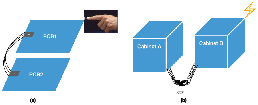
- There needs to be a resonant structure. In electrical terms, this means an undamped/lightly damped L-C circuit. Physically, this could mean anything in an electrical system. Two typical cases are shown in Figure 1. As shown, two PCBs that have a cable connection represent an L-C circuit where the inductive component L depends on the length of the cable and the capacitance component C depends on the structure of the PCBs (areas and the distance between the PCBs). For larger system installations such as the one shown in Figure 1(b), L depends on the length of the ground leads of each cabinet and C depends on the area of the side wall of the cabinet and the distance between the two cabinets.
- There needs to be an excitation source. Translated into EMC terms related to emissions, the excitation source could be any switching source on a PCB or in a system. For immunity, the excitation source could be an external RF field, an ESD event, or a lightning strike, as shown in Figure 1.
- An antenna-like structure can also be treated as a structural resonance depending on the physical size of the conductor. Since an antenna is excited most effectively when the size of the antenna (often a wire) is either one-half or one-quarter the wavelength of the exciting frequency, the physical length of the antenna determines the resonance frequencies.
An analytical approach generally requires experience and technical know-how to model/simulate the system. For small systems with known issues, such as the case study presented in Reference 1, simple mathematical calculations are often good enough to give an estimation of the resonant frequency of the device under test (DUT). Often, an analytical approach is achieved either by 3D full-wave simulation or some specialized EMC software.
The benefit of the analytical approach is that it can make a prediction before a prototype is built, making this approach popular in the design and development of automotive, aerospace, and space applications. Often, such companies have simulation models that have been validated in the past and that can be easily modified for a new study. But for companies that don’t have existing models, building a simulation can be a costly and lengthy journey.
In the time domain, measuring the resonant current with an RF current monitoring probe when a pulse is injected into the system is often used (see Reference 4). This serves as an effective technique when it comes to troubleshooting large systems or where multiple PCBs are interconnected.
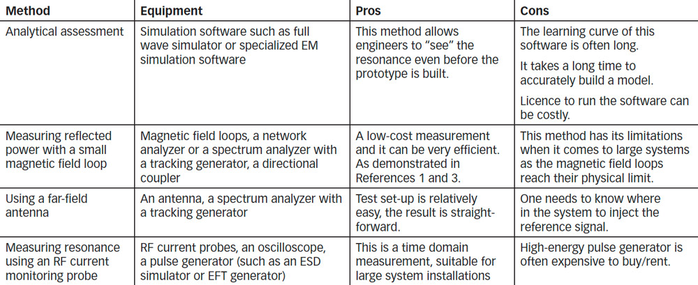
Table 1 summarizes the techniques and pros and cons of each method.
These techniques are introduced and demonstrated in Reference 1. This article further explores more practical approaches based on the characteristics of structural resonances.

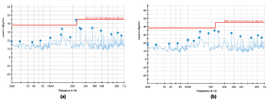
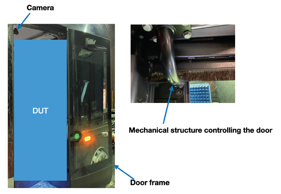
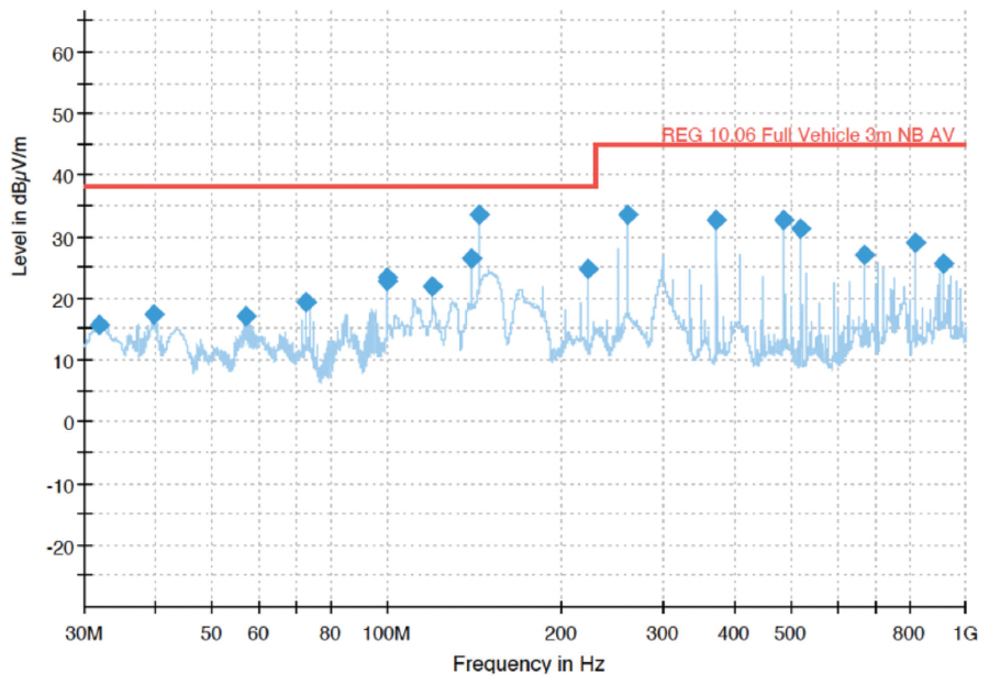
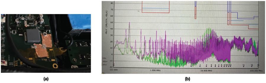
During the radiated emission tests of a large-size electric vehicle, it was found that a narrowband spike at 222MHz exceeded the limit (Figure 2a). It was found that the noise came from a camera that was fitted in the cabin of the vehicle. Multiple ferrites were used on the power leads of the camera, but the improvement was not significant enough to suppress the noise (this is another sign of structural resonances). The test also showed an “inconsistency,” as the same noise was measured a lot lower on some occasions (as shown in Figure 2b). We accidentally discovered that the difference in the emission results was caused by the door of the vehicle. When the door was open, the noise emission was significantly less than when the door was closed.

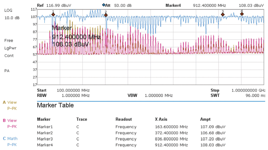
The PCB of the DUT has a size of roughly 50 mm × 50 mm, forming a 200 mm-long loop. The assumption was that traces and tracks on the PCB might have formed an efficient loop antenna within the 200-350 MHz frequency range. Electromagnetic wave travels in an FR4 material at a speed of 1.5×10⁸ m/s, based on equation v=λf, where v is the speed of light in FR4 and f is the frequency. For a 200 MHz wave, a full wavelength is then calculated to be 750 mm. A quarter of wavelength (where the radiation is the strongest) is 187.5 mm. The PCB itself can resonate at a frequency range of 200 MHz. It would probably absorb more RF energy at 200 MHz (and its harmonics) which is injected from the noise source in the immunity tests.
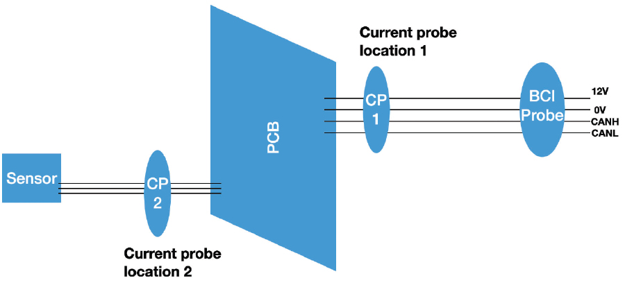
Using an RF current monitoring probe, we measured the RF in front of and behind the PCB in the immunity test, as shown in Figure 5. A frequency sweep was performed from 100 MHz to 1GHz. The RF amplifier injected the same level of RF noise into the main connector cable via a BCI probe from a frequency range of 100 MHz and 1 GHz. The results are shown in Figure 6.
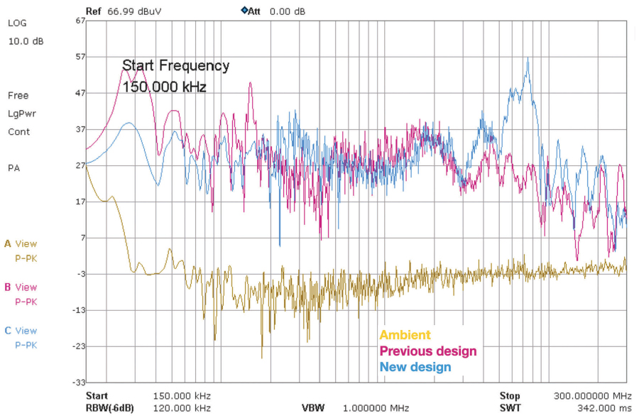
The solution to this immunity problem requires a common mode choke (CMC) that works most effectively in the frequency range of interest, together with decoupling capacitors. The capacitance values are 470pF as they work effectively in this frequency range.
- M. Zhang, “Structure Resonances: Ways To Identify, Locate, and Fix EMI Issues,” Signal Integrity Journal.
https://www.signalintegrityjournal.com/articles/2420-structure-resonances-ways-to-identify-locate-and-fix-emi-issues - D. Smith, “Measuring Structural Resonances,” https://emcesd.com.
- T. Williams, “Controlling Resonances in PCB–Chassis Structures.”
- D. Smith, “Measuring Structural Resonances in the Time Domain,” https://emcesd.com.
- B.R. Archambeault, PCB Design for Real-World EMI Control, Kluwer Academic Publishers, Norwell, Massachusetts, 2002.