Feature Article
Identifying Coupling in Real World Systems
A Beginning Guide to How Noise Moves in a System and How to Stem It
Close-up of a person's hands adjusting the knobs on an oscilloscope or electronic test equipment in a dimly lit lab or testing facility.
U

nintended electromagnetic coupling shows up in more ways than we care to admit. Picture this: your latest PCB assembly comes back from fabrication, you power it up, clip on the scope, load the bring up code, and the screen fills with ragged edges and random spikes. The demo you expected to run clean now looks like a jittery mess, and the system that behaved in simulation suddenly appears unpredictable.

You ask around and hear the classic replies: “That is just noise,” or “That’s just crosstalk.” We have all been there. Those symptoms are almost always attributed to unintentional coupling between circuits, which is energy moving along paths we did not intend to create. The usual suspects are layout choices, component selections, cable and harness effects, or enclosure details that felt minor at the time but that have big consequences during bring up. These decisions generally range from:

  • A slightly long return path, a decoupling choice that looks fine on paper; to
  • A FET gate loop with more area than it should have can be enough to tip a marginal design negative.
This article builds a practical framework you can use on the bench and in the chamber. We will start with how energy moves through a system: conductively through return paths and impedances, and electromagnetically through capacitive, inductive, and radiated paths. We will then separate problems by mode, common mode versus differential mode; that single classification often points directly to the shortest fix. Along the way. we will introduce and align around a simple vocabulary, such that debugging can center around the EMI model: source, path, and receptor, all without talking past one another.
An oscilloscope shot of “noise”
Figure 1: An oscilloscope shot of “noise”
From there, we will examine the most common conducted mechanisms that show up during bring up, including concrete examples and common remedies, plus share notes on how to verify that the change addressed the issue.

Next, we will step into a near field versus far field coupling. We will discuss what changes in the reactive region, why fixes that work on some issues may not work on others, and how to recognize when a local magnetic or electric field interaction is dominating the behavior.

Finally, we’ll lay out a field-tested debug workflow for when someone asks, “Why does the circuit quit working when the motor starts?” The goal is not only to quiet the waveform today, but to give you a repeatable method to identify the path, identify the mode, and remove the coupling with minimal impact on schedule, so you can get back to your product.

Defining Coupling, and the Basic Methods for Energy Transfer
When two parts of a system couple, it simply means energy leaves one circuit and shows up in another. The result can be an unwanted perturbation on a signal, elevated emissions, or failure of the intended function. To understand how that energy moves across a PCB, a module, or a full system, we start with two top-level categories:
  • Conducted coupling: Energy rides on conductors and their return paths. It flows through intentional interconnects and unintended impedances in planes, cables, and grounds.
  • Radiated coupling: Energy leaves a structure as an electromagnetic field and is received by another structure, much like an antenna.
And your problems rarely live in a tidy box, and this results in a spectrum of coupling. Conducted issues travel along wires and planes and through the parasitics that you did not mean to build. Radiated issues depend on the radiating structure, the wavelength, and which field is dominant at the distance of interest. In practice, local capacitive and inductive interactions live in the near field, while true free space wave radiation dominates longer distances. The center of this picture is the crossover (see Figure 2).
The vein diagram of coupling
Figure 2: The vein diagram of coupling
The trust source-path-receiver model
Figure 3: The trust source-path-receiver model
A conducted problem can be the source of a common mode noise onto a cable that radiates strongly. A strong external field can induce a voltage or current on a trace that looks exactly like conducted interference at the receiver.

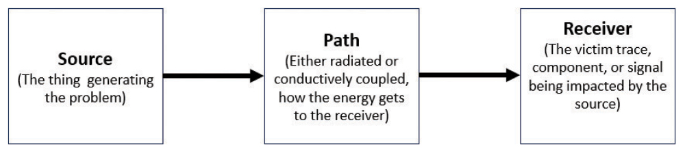
The first step in creating our mental scaffolding is to use the EMC/EMI model, and determine following:

  • The Source of the coupling, often a signal with a fast edge rate such as a PWM drive signal or communications bus.
  • The Path, or how the energy is coupling from the source to the receiver.
  • The Receiver, which is often easily identified as it’s the device that is not delivering its intended function.
Taking this mental model into consideration, we’ll start by examining the path and focus first on conducted coupling by classifying coupled noise currents as common mode or differential mode. That single decision often narrows the root cause and points to the lowest effort fix.
Conducted Coupling: Differential Mode
Conducted coupling in a system shows up through two main mechanisms, differential mode and common mode. In differential mode, the intended current flows out and back on a loop between a source and a load. Any unintended impedance in that loop turns that current into an unwanted voltage. In common mode, the two conductors share a noise current in the same direction with respect to a reference.

We will start with differential mode because it is the easiest to see and the fastest to fix during startup.

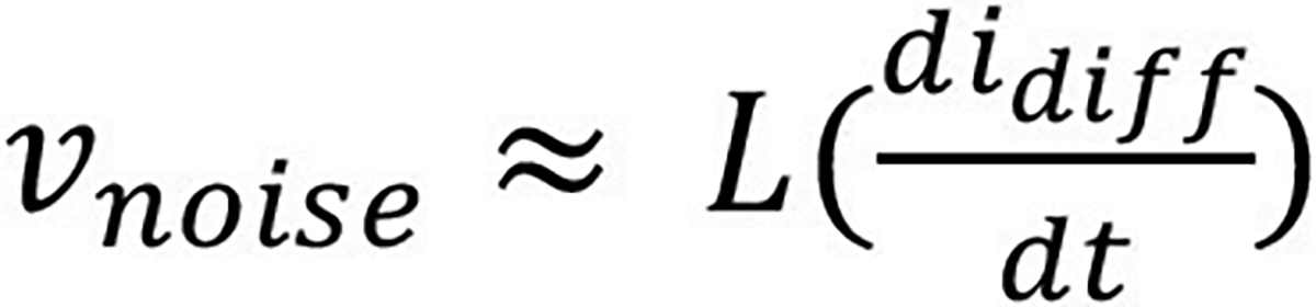
In Figure 4, the intended operating current is labeled idiff. It leaves the power supply, travels through the circuit under test, and returns to the source on its defined return path. Along the way, the loop encounters small but very real impedances in components, vias, traces, planes, and connectors.

The differential mode current model
Figure 4: The differential mode current model
The parasitics of a capacitor
Figure 5: The parasitics of a capacitor
The parasitics of an inductor
Figure 6: The parasitics of an inductor
The parasitics of a trace
Figure 7: The parasitics of a trace
When idiff passes through those impedances, it develops a noise voltage:
  • For resistive elements, the relationship is an IR drop,
Equation 1
  • For inductive elements, the relationship is
Equation 2
  • For capacitive elements, the current that must be the source is
Equation 3
  • , which shows up as extra ripple or ringing in the loop.
Apart from a basic voltage drop, the main takeaways are:
  • The faster you drive current through a series impedance, the greater a voltage error, and
  • The larger the loop geometry, the more susceptibility is created in nearby fields.
Hidden Parasitics
Applying these concepts, we can come up with a list of common sources with parasitics you did not plan for in the intended current path:
  • Capacitor parasitics: The wrong dielectric or package, long pads, or tall stacks push up ESR and ESL. A single X7R 0402 may have about half a nanohenry of ESL; at 100 MHz, that is a few tenths of an ohm, resulting in noticeable ripple. Poor placement lengthens the loop from pin to capacitor and back, which adds trace and via inductance on top of the part’s own ESL.
  • Inductor parasitics: DC resistance (DCR) of an inductor creates a drop under load. Leakage inductance and interwinding capacitance form resonances with surrounding caps. The wrong core material or a part driven into saturation increases effective impedance and injects sharp edges into the loop.
  • Trace and loop parasitics: Narrow neckdowns, long detours, and unnecessary layer changes add resistance and inductance. A via is on the order of a nanohenry. A few millimeters of thin trace can add several nanohenries. With a 1-amp step in 50 nanoseconds, 10 nH makes about 0.2 V of unwanted drop. Split planes or slots that force the return to wander also enlarge the loop and raise the series impedance that the current must cross. Additionally, close routing and high impedances/low currents can result in mutual capacitive coupling both to return and to other traces, injecting noise currents on victim lines.
  • Connectors and cables: Pin assignment, contact resistance, and pin inductance add series impedance. A single, fast, high-current pin next to a sensitive analog pin is a prime example of this.
  • Measurement setup: Long ground leads on a scope probe add inductance and will show ringing that is not on the circuit. The probe can easily become the dominant parasitic in a sensitive loop.
Differential mode coupling is usually correlated with the load current and addressed with decoupling and filtering. You will see supply rails dip or ring when a power stage switches, or a comparator false trigger when a motor phase current steps. The signature often follows the waveform that drives the loop and improves when you shorten the loop or reduce.
Identification and Mitigation of Differential Mode Emissions
The next step in our mental scaffolding is to locate where differential mode emissions arise in a real system. To center the discussion, consider a synchronous buck converter as shown in Figure 8. The goal is to translate an acceptable schematic into a layout that does not amplify parasitics. We will start with a non-optimized layout in Figure 9 and work toward an improved version.
Schematic of a basic synchronous buck converter
Figure 8: Schematic of a basic synchronous buck converter
Layout of a basic synchronous buck converter
Figure 9: A not-so-great layout of a basic synchronous buck converter
When translating from schematic to layout, it’s often difficult to balance the design requirements while mitigating differential mode noise.

Begin at the input. The input capacitors provide local DC stability on VIN. Without them supplying the transient current, every switching event pulls current through the upstream harness, and you will see dips on VIN. In the initial layout, the two input capacitors sit at a noticeable distance from the device.

  • The fix is to reduce parasitics and shrink the current loop. Use several small case multilayer ceramic capacitors right at the VIN pins and the closest return so the mounting inductance is minimal. Parallel values to spread resonances rather than relying on one part to do all the work.
  • Then, shorten and thicken the high current path. Feed VIN with a local plane instead of a long trace, and when a layer change is unavoidable, use multiple vias in parallel to keep the effective inductance low.
We can realize these two concepts and come up with the following, denoted in Figure 10.
An example of improved input capacitor layout
Figure 10: An example of improved input capacitor layout
An example of an improved buck layout
Figure 11: An example of an improved buck layout
Now, focus on the switch loop, which is the phase node between the device switching output, the inductor, and the output capacitor bank. We continue to focus on the copper first, and then move to proper component choices:
  • We strive to keep this loop small and planar, making the copper continuous and wide so there are no skinny neckdowns at device pins or layer transitions that become the dominant impedance. Additionally, we minimize the exposed area of the phase node to reduce its capacitive coupling to nearby nets.
  • Place the first output capacitors as close as practical to the inductor and the return so the AC component of the inductor current closes locally.
  • Additionally, our focus remains on intelligent component choices to minimize parasitic, an inductor that does not saturate at peak current and whose DCR does not waste margin. Use output capacitors that hold value over bias and temperature. Favor packages and footprints that keep pads short and the current path direct. Shielded inductors and careful body orientation reduce stray fields into sensitive nodes.
As you apply these steps to the non-optimized layout in Figure 10, you will see a pattern emerge. Current loops get shorter and thicker, parasitic inductance drops, and the converter becomes easier to probe and control.

With the differential path under control, the remaining noise that shows up at the chamber often comes from hidden common mode currents traveling along cabling and long traces.

Conducted Coupling: Common Mode
While differential mode emissions usually trace to currents you can point to on the schematic, common mode coupling arises when a signal rides on multiple conductors in the same direction with respect to a shared reference, such as a supply, ground rail over an earth connection. Typical symptoms include:
  • Power rail collapse, where a nominally stiff rail shows dips or ripple; and
  • Ground bounce, where the reference no longer holds a steady zero volts.
We will use the common mode model in Figure 12.
The common mode noise current model
Figure 12: The common mode noise current model
In this model, instead of the functional current shown in blue, a common mode current circulates through the system reference. It often originates from parasitic capacitances between fast switching nodes and nearby structures such as planes, chassis, cables, or the environment. As this current returns to its source, any impedance it meets creates voltage that lifts or disturbs the entire reference.

These currents are sometimes called drift currents or antenna currents. They are tricky because the dominant path is geometric rather than schematic, so the loop may involve the PCB layout, a cable shield, and even the test setup, none of which are obvious in the schematic. As with differential mode, we will discuss the impact of common mode coupling on low voltage signaling in CMOS logic.

Common Mode Coupling Impact on CMOS Logic
Input/output voltage signaling has steadily crept down over time, and I/O levels that were once at 5v are now switching at 1.8v, shrinking noise margins.

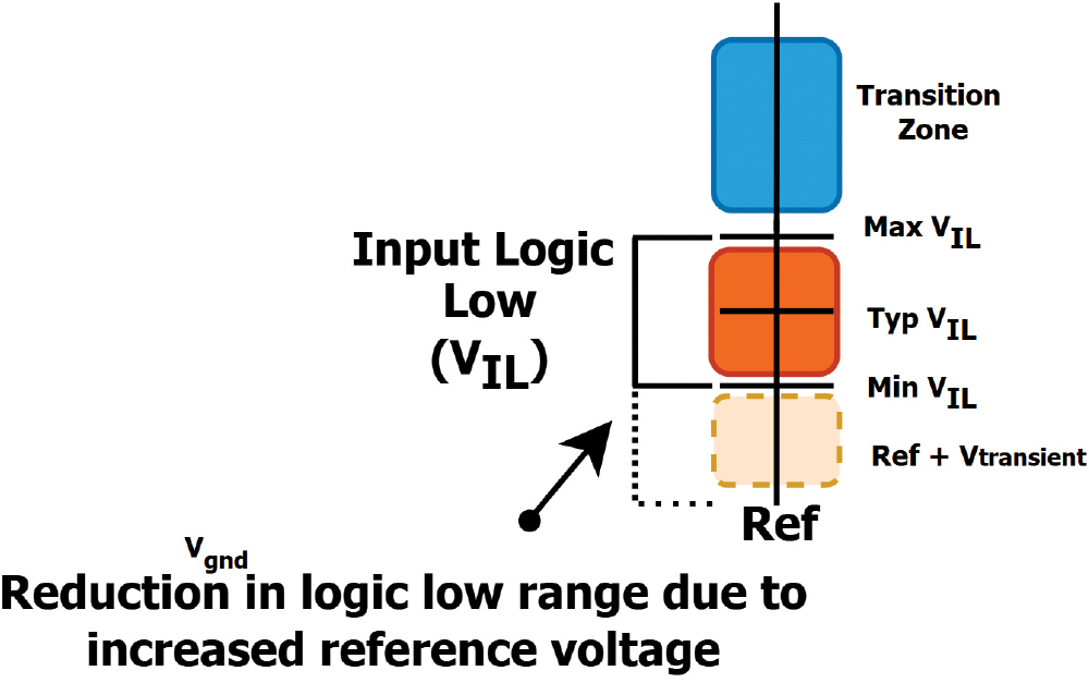
That shrinking margin tightens when the receiver decides on a one or a zero. Specifically for CMOS, the input thresholds voltage input high (VIH) and voltage input low (VIL) are defined relative to the local supply and the local reference; this relationship is shown in Figure 13.

The input output model with basic logic levels for 3v3 logic
Figure 13: The input output model with basic logic levels for 3v3 logic
This logic only behaves if both the supply rail and the reference stay where we think they are. The reference is easy to overlook on a datasheet because it appears under many names, such as AGND, PGND, GND, or AREF. Inconsistent naming resulting in shared return paths can perturb the reference plane. When the reference lifts, the effective thresholds at the input shift, even though the schematic has not changed.

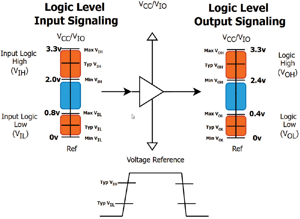
Figure 14 demonstrates this. The reference moves from zero to a transient positive value. That rise reduces the range where the gate recognizes a valid low. With enough bounce, the receiver can miss a low going transition entirely, which shows up as a missed edge in an SPI or I2C transaction. The same mechanism can also create a false height in a gate driver, as shown in Figure 15.

The input low logic level when the reference is lifted by a transient
Figure 14: The input low logic level when the reference is lifted by a transient
A reference plane being lifted to some minimum level during edge transitions
Figure 15: A reference plane being lifted to some minimum level during edge transitions
This is classic common mode behavior. A fast node elsewhere couples through parasitics into planes, cables, or the chassis, launching current that returns through whatever impedance is available. As that current returns, it creates voltage on the shared reference. The receiver does not see the absolute line voltage. It sees line minus reference. If the reference is moving, the apparent level at the pin moves with it. On I2C, where pull ups establish the high level and devices pull down to make a zero, a lifted reference can keep the line above VIL long enough to miss a start, stop, or data bit. On SPI, reference movement can shift both data and clock relative to the threshold, which can violate setup and hold and produce sporadic bit errors; an example of a missed edge is in Figure 16.
A missed edge on a 12C or SPI trace due to a lifted return plane
Figure 16: A missed edge on a 12C or SPI trace due to a lifted return plane
Where Does It Come From, and How to Get Rid of It
While differential mode coupling usually comes from non-ideal elements in the intended current path and is often easy to spot, common mode coupling is trickier. You rarely see the dominant path on the schematic. It is set by geometry, by parasitic capacitances from fast signals into planes, chassis, and cables, and by small imbalances that convert differential energy into a net current on a bundle with respect to reference.

The most reliable way to keep common mode under control is to bake it into layout and system rules from day one.

This includes keeping return paths contiguous so currents can come back directly under their forward paths. Use zoning and floor planning so high current power stages and sensitive interfaces do not force each other across splits or long detours. Place inputs and outputs so they enter and leave the board without crossing cuts in the reference plane, and avoid plane slots that make the return wander. And in systems with long interconnects, treat the cable interface as its own circuit. Terminate shields with a continuous 360-degree bond at the connector or enclosure, not a long pigtail. Provide a local path that brings common mode current back to its source at the point of entry.

A full line filter with common mode, and differential mode counter measures
Figure 17: A full line filter with common mode, and differential mode counter measures
Differential trace routing (left), and an incorrect way that creates imbalanced currents (right), a correction
Figure 18: Differential trace routing (left), and an incorrect way that creates imbalanced currents (right), a correction
Examples of common mode counter-measures
Figure 19: Examples of common mode counter-measures
That usually means a combination of a common mode choke in series with the lines and one or more safety-rated Y capacitors from the lines or reference to chassis or a quiet reference. The choke raises impedance to common mode without disturbing the intended differential signal, while the capacitors give the noise a short return.

Balanced routing matters. Differential pairs and matched lines cancel fields and resist conversion to common mode when their impedances and environments are symmetrical. When the pair becomes unbalanced by skew, uneven reference, neckdowns, or a via only on one leg, that cancellation breaks. The remainder becomes common mode that couples to nearby structures and finds a large path through planes or cables.

Filtering for common mode works because it corrects those imbalances and supplies low impedance returns. At the interface, the common pattern is a line filter that includes a common mode choke close to the connector and short capacitive shunts to the reference or chassis on the board side of the choke. Inside the box, stitching capacitors across unavoidable seams or between local and chassis reference at high frequency give noise current a short loop. Where practical, reduce the

Equation 4
and
Equation 5
of the aggressor with snubbers or control the gate driver parameters so that less energy is driven through parasitic capacitances in the first place.
Identifying the Radiated Nature of a Conducted Coupling Problem
As we move from conducted coupling into radiated effects, remember that many real problems are not clear-cut. Differential and common mode currents that start on copper can excite structures that radiate. Every noise current path can act like an antenna. Our job is to spot it and make that antenna inefficient.

In differential mode radiation, the loop is formed by the intended signal and its return, as shown in Figure 20. The radiated field grows with loop area and with the current edge rate. To manage this:

  • At the module level, the remedy is simple in concept: route high current or fast signal loops directly from source to load while keeping a solid, adjacent return so the loop stays small and planar.
  • At the system level, use twisted pair or a shielded cable so the forward and return currents stay close together and cancel fields.
The differential mode model with loop area being the driving factor in its ability to radiate
Figure 20: The differential mode model with loop area being the driving factor in its ability to radiate
Common mode noise is primarily impacted by the length at which currents must travel to return to their source. Here, long conductors, traces, rails, and especially cables behave like monopole or dipole antennas driven by common mode voltage. The strength of the radiation depends on the length of the structure relative to the wavelength and on the impedance of the return through stray capacitances to the chassis and to space, modeled in Figure 21.
The common mode model shown with cable length being the driving factor in its radiating ability
Figure 21: The common mode model shown with cable length being the driving factor in its radiating ability
Long, unterminated pigtails, breaks in the reference plane, and poor shield terminations make these antennas efficient, and are the low-hanging fruit to be addressed first.

The next section of this article builds on this by mapping the dominant radiated coupling mechanisms and showing how to degrade the antenna that your layout or harness accidentally created.

Radiated Coupling Mechanisms
Radiated coupling is conceptually changing because it asks you to reason about the electric and magnetic fields around a conductor and how those fields change with distance. To help our understanding, imagine you are a neighboring circuit sitting a distance D from a source. What you “see” depends on two things: how close you are and the wavelength of the signal.

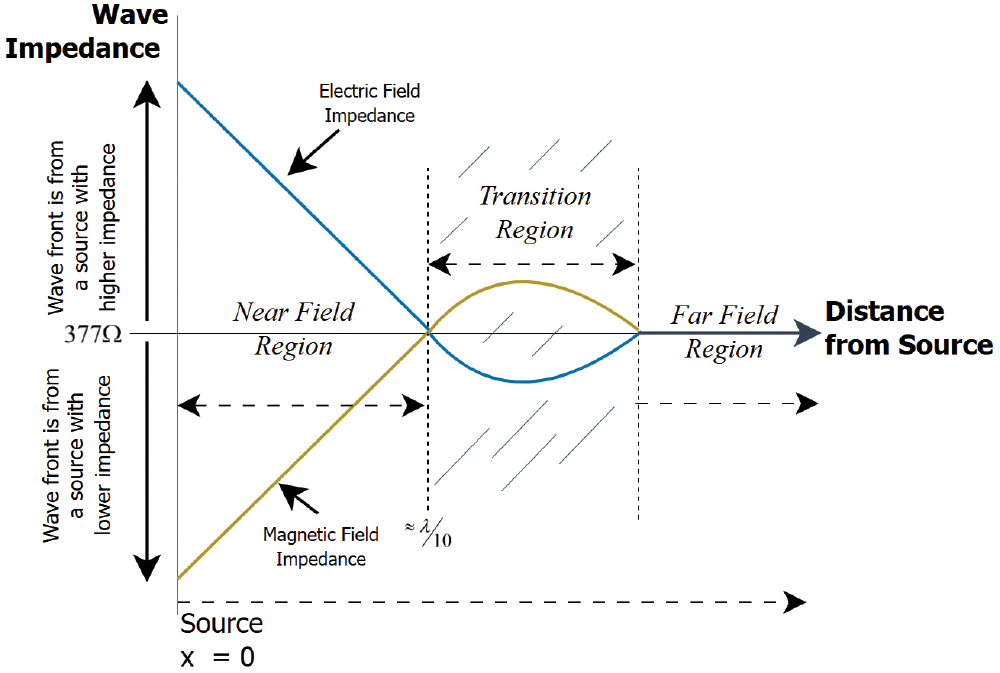
Up close in the near field, the electric and magnetic parts are not locked together. One often dominates the other, with both appearing out of phase. Energy is mostly stored and returned to the source rather than carried away. Farther out, the fields settle into a traveling wave where the electric and magnetic parts are in phase and tied together, and the ratio E/H approaches the impedance of free space (about 377 ohms). Shorter wavelength signals reach this traveling wave behavior at shorter distances. This transition point from the reactive, near field region to far field is thus governed by the following two relationships.

Equation 6
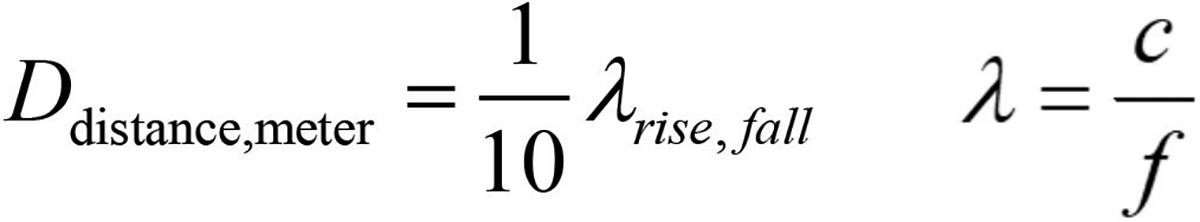
  • For small sources where the physical size
Equation 7
  • , the reactive near field is roughly within
Equation 8
  • (about 0.10-.16 of a wavelength). Beyond that, the fields begin to behave like a radiating wave.
  • For larger structures (enclosures, long cables, big boards) the start of the far field is better estimated by
Equation 9
  • . Here, the size of the radiator matters as much as the frequency.
Practically, that gives us a simple relationship shown in Figure 22.
Wavefront as a function of distance from the source, identifying the three impedance “regions” as it traverses to a 377ohm wave.
Figure 22: Wavefront as a function of distance from the source, identifying the three impedance “regions” as it traverses to a 377ohm wave.
This relationship is described by how close you are to the source. When you are very close to the source, you are in the reactive near field, generated by either:
  • Magnetic sources (current loops) or
  • Electric sources (voltage on small structures).
And these tend to couple through your system in different ways. As you step back to distances on the order of a fraction of a wavelength and you enter a radiating field near region where pattern forms but is not yet settled, you’re entering what is often called the transition region. Step back farther, and you are in the far field where a simple traveling wave description works, and antenna length and orientation are the dominant coupling mechanisms.

Now we’ll focus specifically on near field coupling, defined by either the magnetic or electric field sources.

Near Field Coupling: Magnetic Field
A straightforward way to understand magnetic sources is to use the transformer analogy. Think of the aggressor loop as the primary and the nearby victim loop as the secondary. A transformer works because the two windings are magnetically coupled. Current in the primary creates magnetic flux, and the portion of that flux that links the secondary produces voltage there by induction. Figure 23 shows this relationship.
Thinking about inductive coupling as linking two sections of a circuit together via a gear or water wheel
Figure 23: Thinking about inductive coupling as linking two sections of a circuit together via a gear or water wheel
Think of the inductance that these two entities share as a gear ratio. The size of this coupling gear Lmutual grows when the loops have a larger area (bigger gear diameter), sit closer together (tighter mesh), share more overlap and better alignment (more teeth engaged), and when each loop has a tight return path that keeps its area small and well defined.
Equation 10
To understand how stray magnetic fields can couple into, and then induce voltages in, neighboring circuits, we need to better understand the term flux and how it relates to inductance. At a basic level, the amount of linked flux and the current in a circuit are proportional to each other, with inductance as the proportionality constant; this flux is the “stuff” around a current-carrying conductor shown in Figure 24.
Flux vectors encircling a current flowing down a conductor
Figure 24: Flux vectors encircling a current flowing down a conductor
We can choose to integrate these flux vectors into an area, as shown in Figure 25.
The math that allows you to move from flux vectors to voltage
Figure 25: The math that allows you to move from flux vectors to voltage
We then integrate these flux vectors over an area, as shown in Figure 24. If we assume the area stays constant and the time-varying magnetic field creating the flux is roughly uniform across that shape, we arrive at a more intuitive view of mutual inductance: how voltage, magnetic field, and area are linked together. This can be summarized with the following analogy:

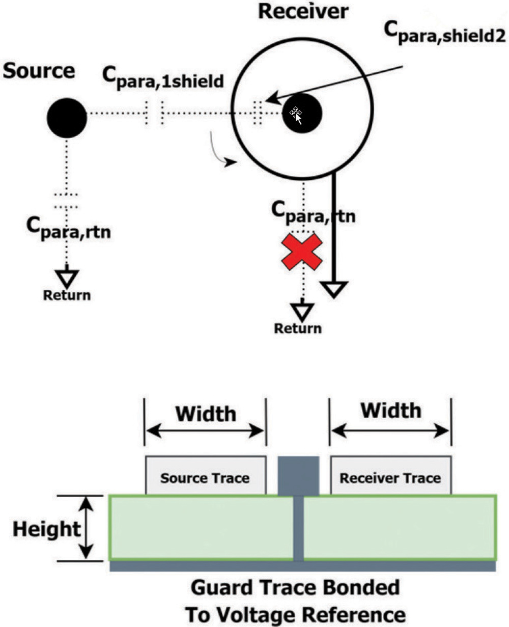
Envision a net, formed by a neighboring circuit, that catches time-varying magnetic field lines, which, through induction, creates a time-varying voltage in that loop.

You can connect this back to the layout and measurement anytime a loop exists. In Figure 26, an inner and outer loop exists, and they’re coupled through the shared flux from the source current’s magnetic field.

From left to right, the transition from loops in a circuit to the equivalent circuit model showing the source and receiver coupled
Figure 26: From left to right, the transition from loops in a circuit to the equivalent circuit model showing the source and receiver coupled
The mutual inductance is shown as linking the source and receiver together, and finally, that induced voltage is then modeled as a frequency dependent voltage source on the receiver circuit or loop.
Near Field Coupling: Electric Field
Similar to the transformer analogy, near field electric coupling can be modeled as a bad antenna or, more precisely, a small open ended capacitor: one plate with charge separated from another plate by a dielectric. In this picture, the source conductor might be a high-speed digital line and the receiver a sensitive analog trace, with air or solder mask separating them, as shown in Figure 27.
The capacitive coupling model
Figure 27: The capacitive coupling model
As the electric field from the source extends into space, it forms capacitance to nearby conductors. One end of that capacitance is the source; the other end is the return plane and the neighboring trace or wire that acts as the receiver. This results in coupling between conductors and between each conductor and its return. These parasitic capacitances couple a source to the receiver in differential mode, and they drive the source and its return together in common mode.

The net effect is a current injected into the neighboring circuit,

Equation 11
as shown in Figure 28. The amount of injected current is set by the mutual capacitance and the source slew or frequency content. The resulting voltage at the receiver depends on its input impedance, including any near end or far end termination, and follows the proportionality that
Equation 12
The equivalent circuit model resulting in an injected frequency-dependent current source in the receiver
Figure 28: The equivalent circuit model resulting in an injected frequency-dependent current source in the receiver
The factors that go into estimating the worst-case parasitic capacitance
Figure 29: The factors that go into estimating the worst-case parasitic capacitance
To control this kind of electric field coupling, we go back to Figure 27 and adjust the few levers we have. Reduce the mutual capacitance by shortening the length that the two conductors run side by side or by increasing their spacing.

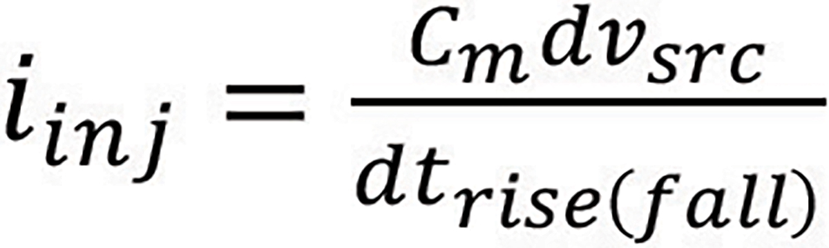
Where possible, reduce the source

Equation 13
or amplitude, though this often has functional tradeoffs.

And while we could next reduce the slew rate or voltage that the receiver is responsible for, that change often impacts the circuit functionally in an adverse way. The goal for mitigation of the impact is to either terminate or shunt the injected current away from the sensitive receiver.

This can result in:

  1. In systems with cables and interconnects, this results in a properly terminated shield. This results in the noise currents being shunted to a common return through a low impedance connection
  1. In PCB systems, guard traces, fencing, along with spacing to reduce and positively impact the parasitic capacitance is found, in addition to orthogonal routing.
These methods are shown in Figure 30.
Managing parasitic capacitance in a cable (left), managing it with guard traces or via fencing (right)
Figure 30: Managing parasitic capacitance in a cable (left), managing it with guard traces or via fencing (right)
In practice, magnetic and electric coupling do not exist apart from each other. The near field exists on a spectrum where loop geometry and frequency often result in problems with mixed signatures. As such, we can refer to Figure 31 to help organize troubleshooting efforts and determine what type of coupling your system is experiencing.
An example of the spectrum of near field coupling
Figure 31: An example of the spectrum of near field coupling
Far Field Coupling
Far field coupling is what you get when the receiver is far enough from the source that the fields behave like a traveling wave. The electric and magnetic parts are in phase, their ratio is about 377 ohms, and the wavefront is close to planar. In this region, long conductors behave like antennas. A cable or trace that carries common mode current looks like a monopole over the reference, with strong radiation near quarter wavelength and its odd multiples. Shorter lengths still radiate, just less efficiently. Field strength scales with common mode current and with the effective length of the conductor and falls with distance.

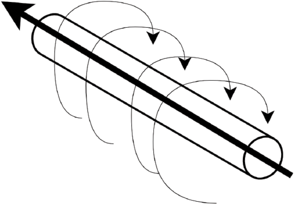
You can picture a driver launching current onto a cable shown in Figure 32.

Current and voltage distribution in a cable (left), how cable drift current takes the electromagnetic return (right)
Figure 32: Current and voltage distribution in a cable (left), how cable drift current takes the electromagnetic return (right)
The cable does not need a separate conduction return to radiate. Energy leaves as an electromagnetic wave, and the “loop” closes locally through displacement capacitance to the chassis and the environment near the source. That common mode current is what the chamber measures when the long cable acts as the antenna.
Conclusion
The next time you have a hard-to-decipher signal on your oscilloscope and a senior engineer says, “You have a coupling problem,” pause before chasing symptoms. Think about how many paths let noise move from one part of a circuit to another.

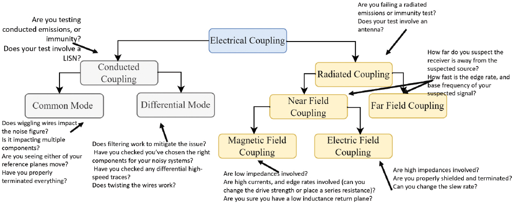
Use the framework you have built and first identify the source, the path, and the receptor; decide whether the dominant mode is differential or common; and check whether a conducted issue has turned into an antenna. Figure 33 is not exhaustive, but it should keep you oriented and help you work through the next problem faster.

The answer to “you have a coupling problem”
Figure 33: The answer to “you have a coupling problem”
Share this story:
Christopher Semanson headshot
Chris Semanson is a Senior Contributor to In Compliance Magazine, and is a Senior Staff Engineer in the systems and solutions team at Renesas Electronics. He has software and hardware experience across a wide range of applications in embedded systems from automotive to inverter management at John Deere and Ford Motor Company. Semanson holds a Master’s degree in Electrical Engineering from the University of Michigan Dearborn, where he studied under Mark Steffka in both computer and electrical engineering. He can be reached at Chris.Semanson.yf@renesas.com.