In Part 8, we evaluated the performance of the baseline AC/DC converter. The baseline AC/DC converter had only the components needed for functionality and did not have any specific EMC components populated. The results showed multiple failures in both radiated and conducted emissions.
Here, we present a systematic approach to improve these failures by populating the PCB with optional EMC countermeasures on component pads that have already been designed into the PCB layout and show their impact on the radiated and conducted emissions. The EMC countermeasures are illustrated in Figure 1 as purple dashed boxes labeled EMC-A through EMC-F.
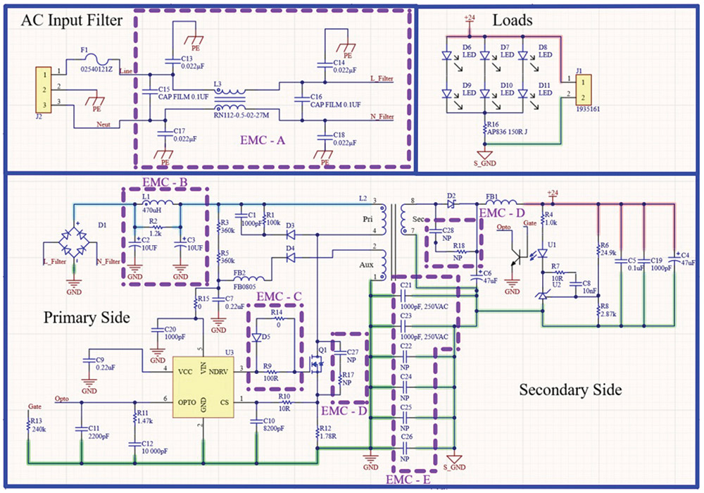
Figure 1: AC/DC schematic with EMC countermeasures
2. Conducted Emissions Results
In an attempt to reduce these emissions, we began with the front-end filtering components (EMC-A) such as Y-capacitors (C13, C17) of the value 0.022µ, between line (L-Filter) and protective earth (PE), and neutral (N_Filter) and PE and an X-capacitor (C15) of the value 0.1µF, between the line and neutral.


Conducted emission results legend
The conducted emissions measurement taken with these countermeasures populated is shown in Figure 2b.
As the plot in Figure 2b shows, the capacitors decrease the emissions by 4-15 dB, over the entire frequency range. There was only one quasi-peak failure at 255 kHz (still reduced by about 5 dB from baseline). There are still several failures over a broad range of frequencies when measured with the average detector.
Next, a Schaffner RN112-0.5-02-27M common-mode choke (L3) was added. The results are shown in Figure 3.
The addition of the common-mode choke eliminated the quasi-peak failure and lowered the emissions mainly below 1 MHz. It may be possible with further study to reduce conducted emissions by evaluating different common-mode chokes. However, we chose to focus on other EMC design controls to make further reductions.


The main impact of the gate resistor was above 1 MHz, resulting in a 2-5 dB reduction in emissions. Further adjustments to the gate resistor R9 or R14 were not evaluated in conducted emissions, pending the measurements of radiated emissions.
Next, the Y capacitor values (C13 & C17) were increased from 0.022 µF to 0.033 µF (EMC-A). The results are shown in Figure 5.
This change eliminated the remaining conducted emissions failures.
Radiated emissions were measured in the frequency range of 30 – 300 MHz. As we have already identified the countermeasures that need to be added to resolve conducted emissions failures, we start radiated emissions diagnostics with all of the required CE modifications populated as per Figure 5. Figure 6a shows the baseline results (DUT with the conducted emissions modifications).
In order to reduce the failing emissions further, two stitching caps (EMC – E) C21 and C23 of the value 1000 pF were added. The stitching capacitors tie the secondary back to the primary at high frequency, allowing noise currents to return to their source more directly rather than through the air, thus reducing the radiated emissions. The result was the reduction in emission, as shown in Figure 6b.
At this point, failures can still be observed in the vertical emissions between 30MHz – 35MHz, and the margin of the emissions around 35-40MHz and 80MHz isn’t sufficient. We typically want to see at least a 6dB margin to the required emissions limit to account for lab-to-lab variation and component/build tolerances. Therefore, a snubber was added across the Drain to Source pin of the switching MOSFET Q1 (EMC – D) consisting of R17 = 10 Ω, C27 = 330 pF to further reduce the emissions. The results are shown in Figure 7.


The addition of the snubber resulted in the device passing the radiated emission test with sufficient margins. The cumulative changes resulted in passing both conducted & radiated emissions results. Front end filtering through the use of X and Y capacitors along with a common mode choke provided a significant improvement in conducted emissions. Adjusting the Q1 gate resistor, adding a snubber across Q1 Drain-Source and stitching capacitance all made significant improvements in radiated emissions. If further radiated or conducted emissions reductions were needed, some experimentation with R14 (turn off Q1 gate resistance) could be evaluated. All design changes are recommended to be evaluated for potential design trade-offs with other requirements such as thermal power dissipation, functionality over temperature and input voltage variations as well as other EMC requirements (including immunity).
- Adamczyk, B., Mee, S., Koeller, N, “Evaluation of EMC Emissions and Ground Techniques on 1- and 2-layer PCBs with Power Converters,” Parts 1-8 available on https://incompliancemag.com.


