he JEDEC/ESDA charged device model (CDM) test standard JS-002 places a component in a metal/dielectric test fixture and uses a field-induced air discharge to test each pin of the component. Current waveforms depend on the circuitry under test, yet are fairly consistent for the small and large CDM verification targets, metal disks specified by JS-002. Those waveforms often fit a simple 2-pole RLC circuit model as shown in Figure 1, and as summarized in our 2014 paper [1].

Our recent EOS/ESD Symposium paper [2] discussed this history, including recent attempts to model waveforms with a variable spark resistance R(t), and our own contribution to that. Details and important references are in [2]. We became more comfortable with the idea of inductance built into the spark once we saw some 2021 work about agricultural sparks, which are much larger than semiconductor CDM sparks. In addition, a plot of (electric and magnetic) field energy vs. time for a typical CDM spark (see Figure 2) shows the expected collapse of field energy into the spark followed by a return of some energy to the field at around 1.5-2 nsec. There must be some kind of energy storage (i.e., a reactive element in the spark) for this to happen. The bump does not vanish for any reasonable values of L and C in the CDM test fixture.


 and is commonly called the damping factor. The waveform will invert into the time domain (Heaviside inversion, in many math books) as a damped sinusoid (D<1), with a complex conjugate pole pair, or as a double exponential (D>1). Our usual case for CDM targets is D<1. But, as indicated above, the large target waveform does not fit the two-pole model of [1,2] very well beyond the first half cycle.
There are essentially two adjustable parameters in Equation 1, since the current can be integrated to give Q=CV0, and C if V0 is known. If only Q is known, the unitary solution (integral=1) is best expressed through variables ω0 and D, as follows.
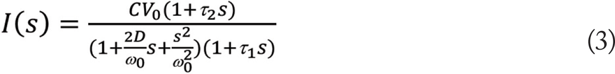
In order to get better fits to our waveforms, and to allow for more reactive circuit elements, we expanded the I(s) current function as simply as possible, by adding a real pole and a real zero:
Heaviside expansion into the time domain of a three‑pole, one-zero (3p1z) model, such as Equation 3, takes the form:

We found 3p1z solutions for several dozen waveforms, mostly from small and large CDM verification targets from my co-authors at Intel and Thermo Fisher. R2 was at least 0.95 and usually well above, and the benefits of two more fitting parameters were clear. Details are in [2]. Next, we sought a one-to-one correspondence between a circuit model and the s-domain expression as in Equation 3. The problem with adding an extra inductor to the circuit in Figure 1 was that τ2>τ1 was not what we had observed. The key insight was to add an extra capacitor and to allow the extra inductance to be lumped in with the probe and fixture inductance. The new circuit is in Figure 3, with the CDM spark elements on the right-hand side, sharing inductance with the probe and fixture on the left. The 3p1z current function is as follows:


![Figure 6: Circuit model and 3p1z parameters for a small, low inductance probe (1 nH) target from a 2023 paper [3], +10V](https://digital.incompliancemag.com/asset/2025/01/circuit-model-fig06.jpg)
This initial work on the CDM spark circuit model should be continued on to larger and smaller target (i.e., package) sizes, and varying probe inductance so that the variety of CDM test and use conditions is comprehended. At some point, trends for all the circuit elements should be clear enough that the circuit model for any metal target (akin to a short circuit) in any CDM environment can be predicted, and with it trends for peak current and such. The model can then, for example, be used as a CDM “source,” surrounding a known ESD circuit model of a pin under test.
To facilitate the exploratory studies of these various CDM test conditions, the algorithm described here and in [2] could be ported to a software platform where the circuit parameters are found after very few keystrokes, as with existing ESD waveform evaluation software for human body model (HBM). Also, now that we have a circuit topology for the spark, we can imagine using a licensed version of SPICE simulator that finds optimized circuit element values given a topology. Having made fast work of the waveform evaluation, we can expect considerable physical insight to emerge from the trends discernable from large amounts of CDM data, much of which is already on file.
Finally, we should see if air spark plasma conditions produce the occasional high-frequency resonance (Figure 6) when certain external L-C conditions are met. This could represent a worst case for CDM peak current in factory assembly/test or D2D conditions. If the idea of an avalanche process and drift time of carriers to anode/cathode resonating with an external circuit sounds familiar to an electrical engineer, it could be because the decades-old high-power microwave IMPATT diode (impact ionization avalanche transit time) works on exactly that principle. We should find out if the occasional occurrence of such conditions is a threat to our devices in manufacturing and protect them accordingly.
- T. Maloney and N. Jack, “CDM Tester Properties as Deduced from Waveforms,” IEEE TDMR-14, pp. 792-800. https://bit.ly/2VQlUfQ
- T. Maloney, P. Ensaf, and M. Hernandez, “Intrinsic Inductance and Time-Dependent Resistance of the FI-CDM Spark,” 2024 EOS/ESD Symposium Proceedings, paper 2B.3, pp.93-102. Paper and slides at https://bit.ly/3WV9nod, slides presented at https://youtu.be/Oa5BQVCFBAo.
- D. Johnsson, P. Tamminen, D. Oy, T. Viheriakoski, H. Gossner, “Discharge Waveforms of Emulated Die-to-Die ESD Discharges,” 2023 EOS/ESD Symposium Proceedings, paper 1A.5, pp. 47-55. https://doi.org/10.23919/EOS/ESD58195.2023.10287762
- P. Tamminen, private communication.

He can be reached at tjmaloney@sbcglobal.net.