hot topics in ESD

Two-Pin HBM Testing: a New Option?

H

uman Body Model (HBM) is the original ESD test method for semiconductor devices and is still the most widely used ESD test [1]. This article will discuss the old, but now new two-pin HBM tester. Not only are the new two-pin testers not subject to one of the drawbacks of today’s high pin count testers, they provide additional testing convenience and diagnostic options not available in traditional HBM testers.

Background
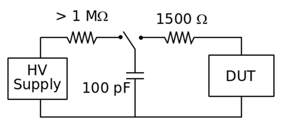
The basic HBM circuit diagram is shown in Figure 1. A 100-pF capacitor is charged to a voltage and then discharged across the device through a series 1500-ohm resistor. This produces the classic HBM waveform, a rapid rise in current followed by a 150 ns exponential decay, with a nominal peak current of about VHBM/1500 ohms. Developing an HBM tester based on Figure 1 is not as straightforward as it might seem. Details of the high voltage relay to initiate the pulse have led to unintended consequences and false failures which have been documented in the literature. Ionized gas in the relay after the pulse created sustained low currents after the main pulse [2] and rapidly changing relay capacitance created voltages before the pulse [3]. These artifacts have been rectified with simple modifications of the pulse source.
The basic HBM circuit diagram
Figure 1: Basic HBM circuit model where DUT is the device under test, conventionally an IC package
Delivering the pulse to the device under test (DUT) can also be a challenge. The very earliest HBM tester was undoubtedly a very simple RCL circuit with a pair of clip leads, a Two Pin Tester. As integrated circuits became more complicated, the test method evolved. To save test time, pin combinations were developed in which a number of pins were ganged together on the low side of the pulse source, while a single pin was stressed on the high side of the pulse source. These are the traditional pin combinations, now in Table 2B of JS-001. [4] To accommodate these pin combinations HBM testers were designed to facilitate the pin combinations in both manual and automated, relay-matrix based, configurations. Relay matrix-based testers have been the mainstay of HBM testing of high pin count for some time, but there have occasionally been issues related to parasitic circuit elements within the matrix, which have resulted in false failures. The next section will discuss how parasitics can lead to distorted waveforms. We will then discuss how a new generation of the two-pin testers has come on the market, such as the Grund Technical Solutions Pure Pulse HBM system and HPPI’s HBM option for their Transmission Line Pulse (TLP) systems. These systems are insensitive to tester parasitics but have a number of other advantages that will be discussed.
Tester Parasitics
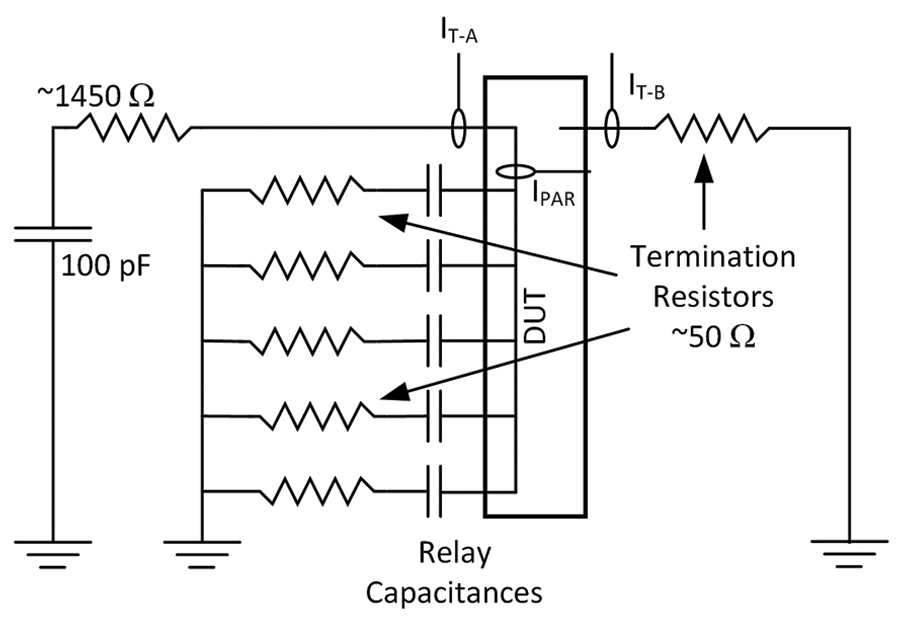
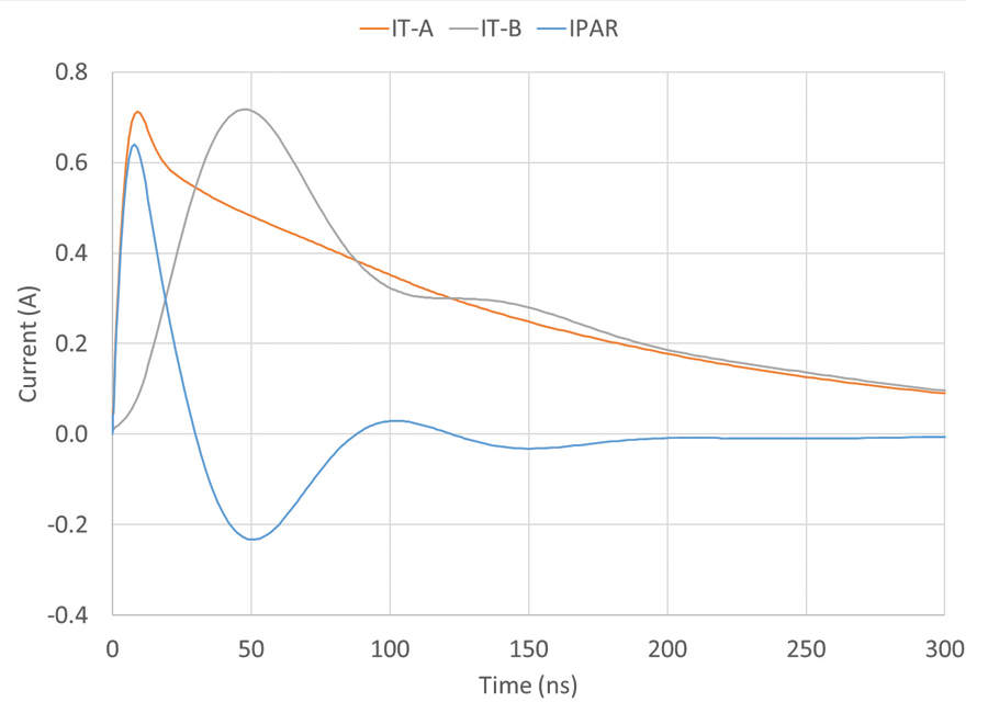
Relay matrix-based testers have been found to have significant parasitic circuit elements, particularly the capacitance across open relays [5,6]. An example is shown in Figure 2 on page 46. If the stressed pin is a supply group with many pins, or an Input or Output with diodes to a power rail, many open relays with parasitic capacitance will be stressed. The result can be that the actual waveform exiting the DUT can be significantly distorted, as shown in Figure 3. The resulting stress waveforms to the ESD protection structures can be very different from the waveform they were designed for and any waveform they would see during handling, which can result in false failures during testing.
The New Two-Pin Testers
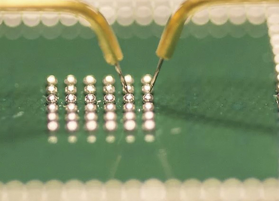
The new two-pin testers deliver the HBM pulse to the DUT using wafer probes, as shown in Figure 4. The Pure Pulse system from Grund Technical Solutions (GTS) system [7] uses RF probes, providing a controlled impedance down to a few mm from the DUT. The HPPI systems, HBM-S1-B and HBM-TS10-A [8], place the pulse source close to the DUT, permitting more conventional cables. By applying the HBM stress directly between two pins on the DUT there are no unintended circuit elements to distort the stress waveform. This ensures that the DUT receives the intended stress. This is, however, not the only advantage of two-pin testers.

The use of wafer probes for pulse delivery has obvious advantages. HBM testing can be done conveniently at both wafer and package level. At the package level, there is no need for a socket, eliminating the cost, design effort, and time delays that are often associated with HBM testing.

Circuit diagram showing a relay matrix based HBM tester

Figure 2: Circuit diagram showing how a relay matrix based HBM tester can have unexpected parasitic capacitance.

Leakage or curve trace measurements before and after HBM stress to quickly detect a signature of device damage has long been a feature of HBM test systems, and two-pin testers include that capability. The two-pin testers go beyond that capability by measuring voltage across the DUT and current through the DUT DURING the HBM pulse. This creates an entirely new level of diagnostic capability for HBM [9].
Line graph depicting simulation of current waveform
Figure 3: Simulation showing that the current waveform out of the DUT, IT-B, may look very different than the input waveform, IT-A due to unintended currents within the device, IPAR, due to parasitic capacitance of relays within the matrix. Refer to Figure 2 where these currents are monitored.
Closeup image of 50-ohm wafer probe needles as part of a two-pin HBM tester
Figure 4: 50-ohm wafer probe needles as part of a two-pin HBM tester.
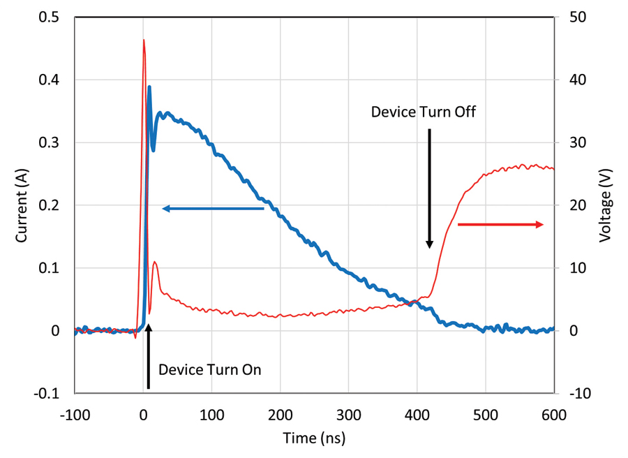
Figure 5 shows an example of the current through, and voltage across, a high voltage device with snapback, stressed with a 750 V HBM pulse. On first inspection, the current pulse looks very much like a standard HBM current pulse through a short. The decay, however, doesn’t quite look like an exponential decay with a 150 ns time constant. At about 420 ns the current drops significantly and is essentially zero by 500 ns. The voltage across the device gives insight into the device’s behavior. At the beginning of the voltage pulse, the voltage rises rapidly, as would be expected for a high voltage device. The voltage rise also starts a few ns before the current. This suggests that there is a delay in current, until the voltage reaches the device turn on above 25 V. The voltage then drops rapidly as the device goes into snapback, and the current starts to behave as an HBM pulse. Voltage reaches a minimum at around 200 ns, rising slowly until 420 ns. At 420 ns the voltage begins to increase rapidly, reaching a peak of 26 V around 550 ns. The rise in voltage corresponds to when the current significantly drops. This indicates when the device leaves snapback and the voltage returns to above its breakdown voltage.

Measuring voltage across a DUT during the pulse also makes it possible to capture the exact time of failure. Device failure is often accompanied by an abrupt drop in voltage across the DUT.

There has been occasional criticism of the GTS Pure Pulse system that it is not a true 1500-ohm source impedance but is a 50-ohm source delivering an HBM current waveform. This is not valid. The waveform is formed using an RCL network similar to those used in a matrix-based tester, which is then delivered over a short 50-ohm line. The situation is actually the same in a matrix-based tester. The pulse is formed with an RLC circuit but is then delivered to the DUT over a series of traces and connections which all have characteristic impedances that are certainly not 1500 ohms but are not as well controlled as using RF probes.

The single area where two-pin testers create a challenge for the test engineer is the implementation of the pin combinations in JS-001 for a two-pin tester. That could be the topic of a future article.

Line graph showing readings of a High voltage device with snapback stressed with a 750 V HBM pulse
Figure 5: High voltage device with snapback stressed with a 750 V HBM pulse
Summary
The new two-pin testers provide an interesting option for HBM testing. They can perform HBM testing at both package and wafer level, and with robotic probe holders, they can perform automated testing. In addition to measuring leakage currents before and after stress, the new testers can measure voltage and current during the HBM stress itself, giving new insight into device performance during an HBM stress. Matrix-based HBM testers have served the industry well and will continue to be a major tool for years to come. They have the advantage of being able to directly use the pin combinations in JS-001’s Table 2A and Table 2B. It is very advantageous, however, to have another option for performing HBM testing without the cost and time required for designing custom boards, as well as a method that is essentially free of the issues of tester parasitics.
References
  1. ANSI/ESDA/JEDEC JS-001-2017, “For Electrostatic Discharge Sensitivity Testing Human Body Model (HBM) – Component Level.”
  2. Duvvury, et al., “Gate Oxide Failures Due to Anomalous Stress from HBM ESD Testers,” EOS/ESD Symposium, 2004, pp. 132 – 140.
  3. Ashton, et al., “Voltages Before and After HBM Stress and Their Effect on Dynamically Triggered Power Supply Clamps,” EOS/ESD Symposium 2004, pp. 153 – 159.
  4. R. Ashton, “HBM Pin Combinations,” In Compliance Magazine, December 2019.
  5. H. Kunz, R. Steinhoff, C. Duvvury, G. Boselli, and L Ting, “The effect of high pin-count ESD tester parasitics on transiently triggered ESD clamps,” 2004 Electrical Overstress/Electrostatic Discharge Symposium.
  6. M. Chaine et al. , “HBM tester parasitic effects on high pin count devices with multiple power and ground pins,” 2006 Electrical Overstress/Electrostatic Discharge Symposium.
  7. Grund Technical Solutions (GTS), Pure Pulse, https://www.grundtech.com/purepulse.
  8. High Power Pulse Instruments (HPPI), Two-Pin HBM Tester, https://www.hppi.de/files/HBM-S1-B.pdf and https://www.hppi.de/files/HBM-TS10-A.pdf.
  9. R. Ashton, S. Fairbanks, A. Bergen, and E. Grund, “Electrostatic test structures for transmission line pulse and human body model testing at wafer level,” 2018 IEEE International Conference on Microelectronic Test Structures (ICMTS).
Share this story:
Robert Ashton headshot
Robert Ashton is the Chief Scientist at Minotaur Labs. He received his BS and PhD degrees in Physics from the University of Rhode Island. Robert is an active member of ESDA working groups for device testing standards and the JEDEC latch-up working group. He has been a regular member of the EOS/ESD Symposium technical program committee.
ESD Association black logo
Founded in 1982, EOS/ESD Association, Inc. is a not for profit, professional organization, dedicated to education and furthering the technology Electrostatic Discharge (ESD) control and prevention. EOS/ESD Association, Inc. sponsors educational programs, develops ESD control and measurement standards, holds international technical symposiums, workshops, tutorials, and foster the exchange of technical information among its members and others.