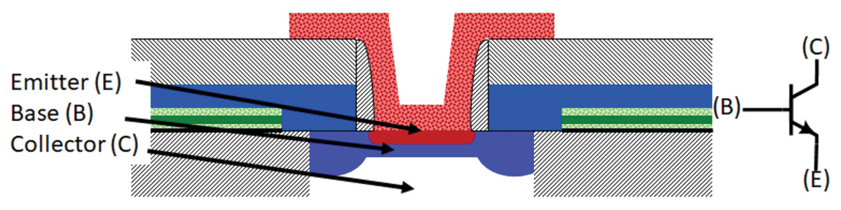
ince its invention in 1947 at Bell Labs by William Shockley, Walter Brattain, and John Bardeen, the bipolar transistor has been implemented in multiple key applications successfully. Nowadays in the semiconductors industry, the bipolar transistor is massively used for various functions in modern integrated circuits (ICs) products. For on-chip electrostatic discharge (ESD) protection solution, the bipolar junction transistor, represented in Figure 1, is a very effective and valuable ESD device. With high ESD performance, low leakage, low input capacitance, and compactness, it has a smaller footprint advantage compared to other ESD devices. Furthermore, modern bipolar devices are reaching record RF performance including but not limited to a high transition frequency fT > 300GHz and minimum noise figure NFMIN < 1dB.
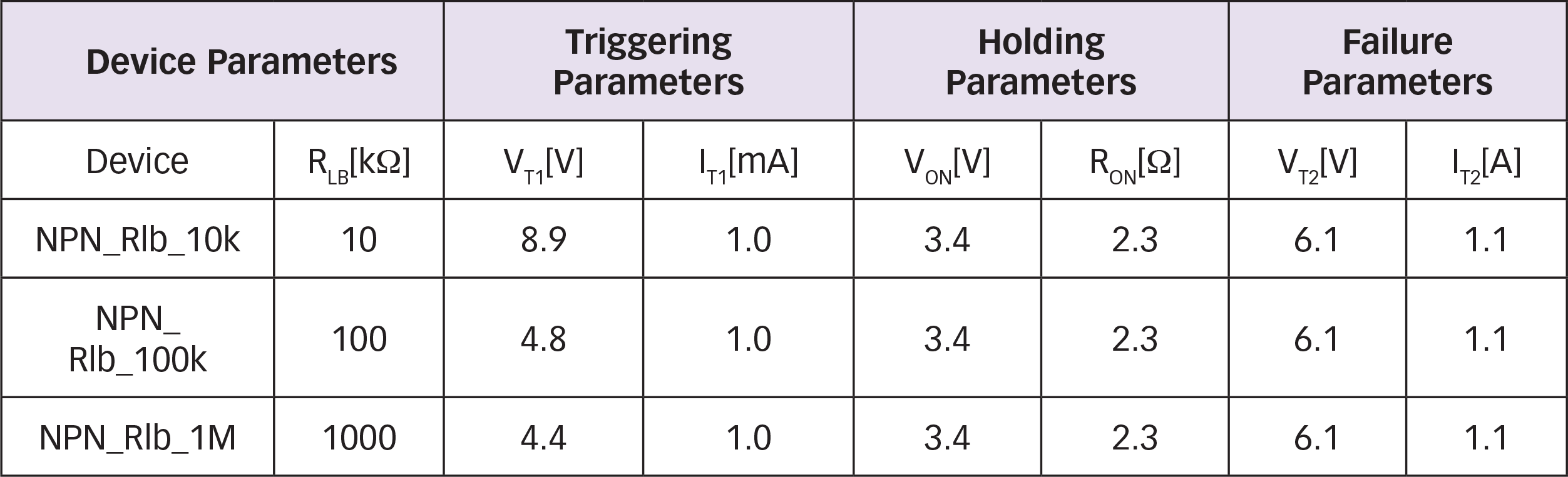
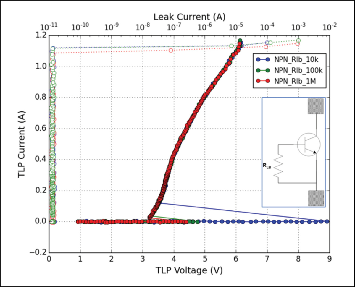
In this example, the standalone latch-back bipolar NPN transistor can withstand up to 1.1A transmission line pulse (100ns-TLP), this is equivalent to about 2kV human body model (HBM) robustness in terms of energy content as shown in Figure 2.
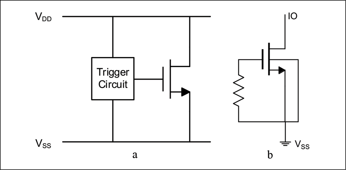
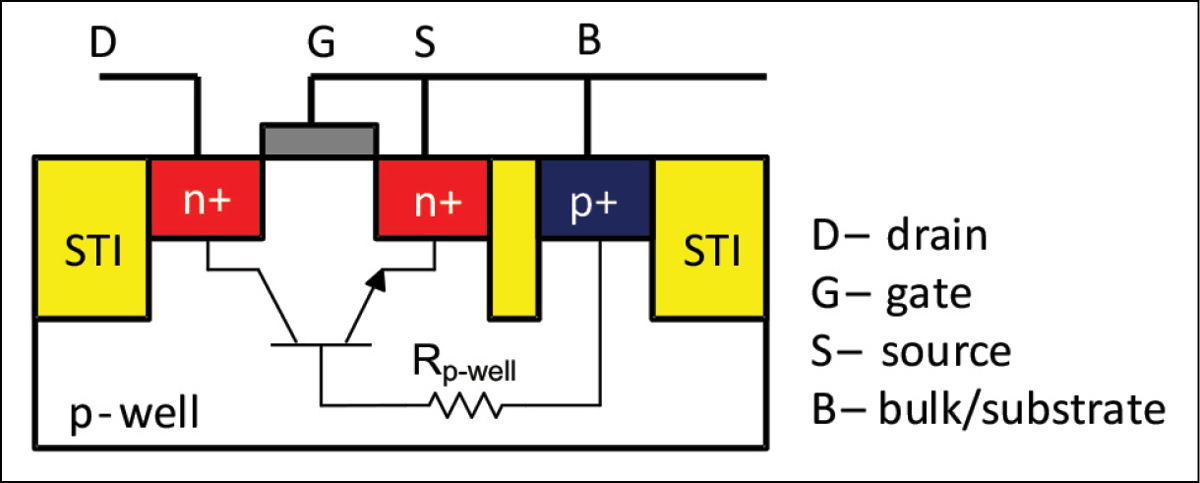
In a power clamp, a transient trigger circuit biases the gate of the “big MOS transistor” for the duration of the ESD current. The MOS-channel provides the low-ohmic path to ground. During normal operation, the trigger circuit keeps the gate closed and the ESD clamp off. In a grounded-gate configuration for a MOS transistor, a high value resistor connects gate, source and bulk. This prevents the biasing of the gate and opening of the MOS channel during ESD stress and normal operation. However, during ESD stress the parasitic bipolar transistor between drain and source (Figure 4) turns on and provides a path to ground for the conduction of the ESD current.
- Dolphin Abessolo-Bidzo et al., “A Silicon BJT Active ESD Clamp Design in a Silicon Germanium HBT BiCMOS Technology,” Electrical Overstress/Electrostatic Discharge Symposium Proceedings, paper 4A.1, 2021.
Dr. Ir. Dolphin Abessolo-Bidzo is Senior Principal RF ESD & Latch-Up Design Engineer at NXP Semiconductors.
Dr. Mirko Scholz is a Principal Engineer ESD Development at Infineon Technologies AG in Neubiberg/Germany.
Marko Simicic is part of the ESD team in imec, Belgium, with the focus on researching ESD solutions for devices and circuits.