EMC concepts explained
EVALUATION OF EMC EMISSIONS AND GROUND TECHNIQUES ON 1- AND 2-LAYER PCBs WITH POWER CONVERTERS
Part 3: DC/DC Converter – Baseline EMC Emissions Evaluation
T

his is the third article in a series of articles devoted to the design, test, and EMC emissions evaluation of 1- and 2-layer PCBs that contain AC/DC and/or DC/DC converters, and employ different ground techniques [1, 2]. In this article, we evaluate the performance of the baseline DC/DC converter (e.g., use only IC vendor recommended components and no additional EMC countermeasures). Specifically, we present the test results from the radiated and conducted emissions tests performed according to the CISPR 25 Class 5.

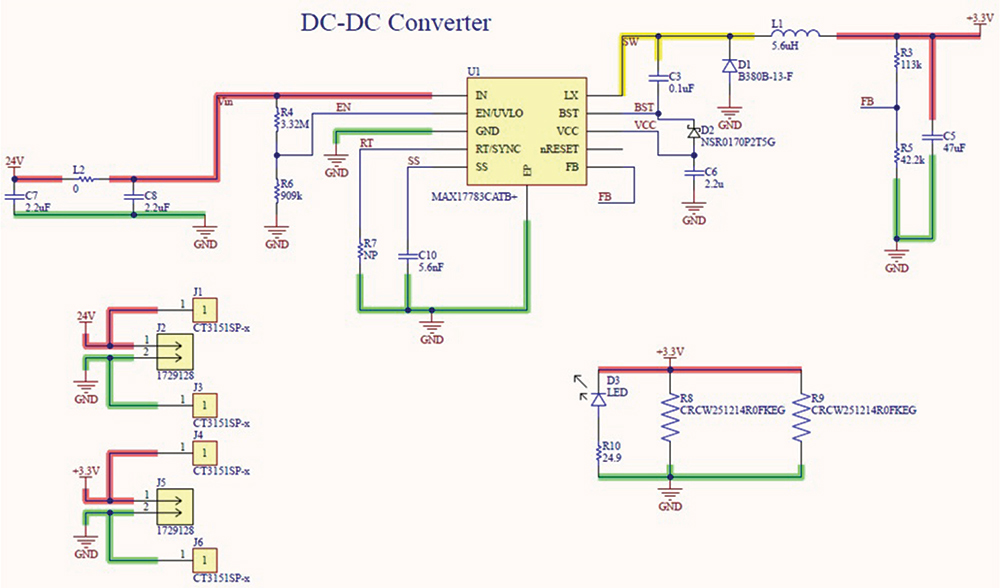
Like so many industries at this time, while working on the DC/DC converter we were faced with a semiconductor shortage issue in our design with the main controller integrated circuit. This forced us to redesign the converter using a different DC/DC IC that is widely available in quantities. After selecting a new integrated circuit, a new design was created and appropriate components were chosen. Then the PCB layout was updated and a ‘quick turn’ PCB fabrication was ordered and received. The schematic, PCB layout, and a photograph of the assembly are shown below for the new design which was tested and results are discussed in this article.

1. Introduction
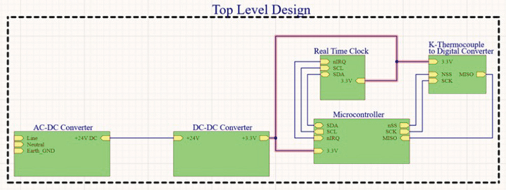
In the first article in the series, [1], we presented the schematic for the overall system shown in Figure 1.

The second article, [2], focused on the details of the DC/DC converter design.

Top-level schematic graph
Figure 1: Top-level schematic
Due to the aforementioned semiconductor shortage, a new design was created using the same process and is shown in Figure 2.
DC-DC converter baseline schema graphtic
Figure 2: DC-DC converter baseline schematic
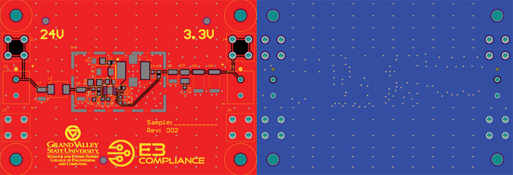
The layout of the DC-DC converter is shown in Figure 3.
DC-DC Converter layout (Top Layer in Red, Bottom Layer in Blue) figure
Figure 3: DC-DC Converter layout (Top Layer in Red, Bottom Layer in Blue)
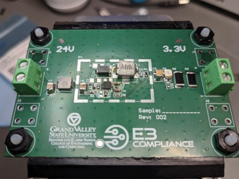
The baseline converter is shown in Figure 4.

This article is organized as follows. Section 2 presents the radiated emissions test results. In Section 3, the conducted emissions (voltage method) results are shown. The current method, conducted emission results are included in Section 4. Section 5 addresses the content of the next article.

DC-DC converter assembly closeup
Figure 4: DC-DC converter assembly
2. CISPR 25 Radiated Emissions Test Results
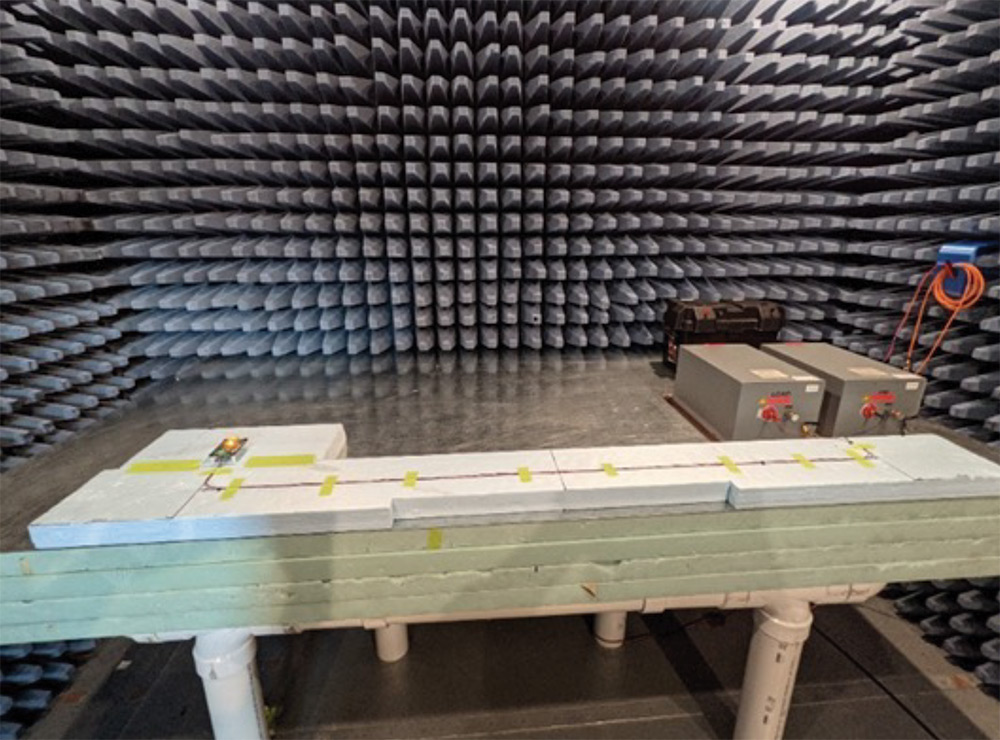
The DC-DC switcher was tested according to CISPR 25 4th Edition, Class 5. The radiated emissions test setup is shown in Figure 5.
Radiated emissions test setup room
Figure 5: Radiated emissions test setup
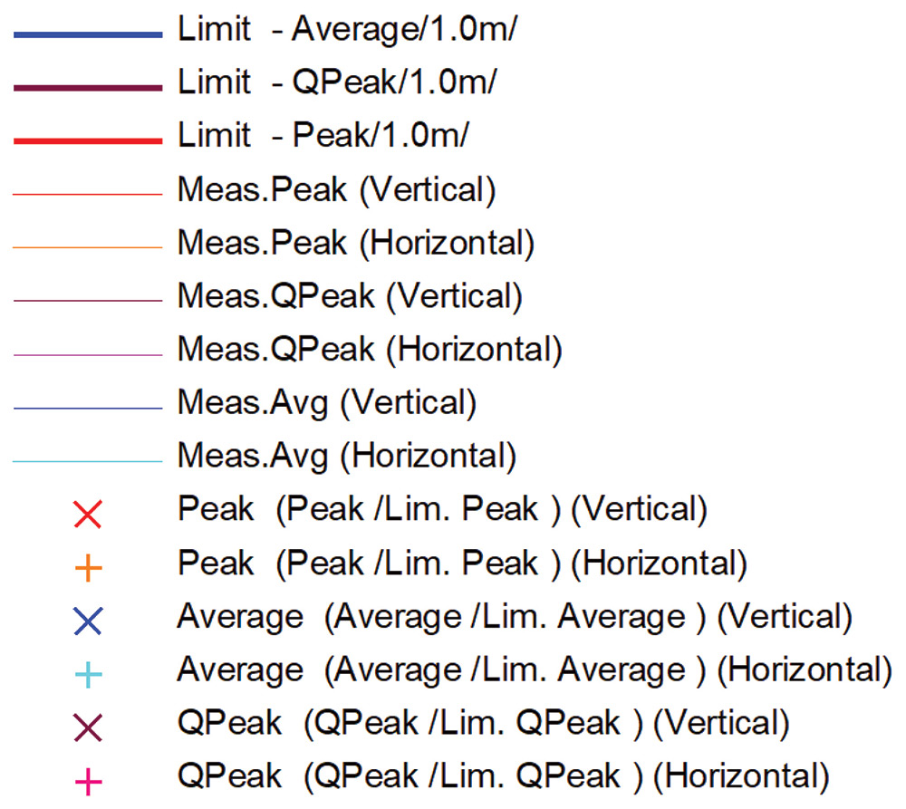
A legend for the radiated emissions plot is shown in Figure 6.
Radiated emissions legend list
Figure 6: Radiated emissions legend
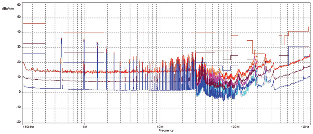
Figure 7 shows the radiated emissions measurements results in the frequency range of 150 kHz – 1GHz. These measurements were made using a monopole antenna from 150 kHz – 30 MHz, a biconical antenna from 30 MHz – 300 MHz, and a log-periodic antenna from 300 MHz – 1GHz.

The monopole range (150 kHz – 30 MHz) shows a failure of the Quasi-Peak and Average limits at 978 kHz and 1469 kHz. The emissions in this region are all narrowband, and spaced by ~487 kHz. This suggests that these emissions are all harmonics of the 487 kHz switching frequency of the power supply.

Radiated emission results in the frequency range 150kHz – 1GHz graph
Figure 7: Radiated emission results in the frequency range 150kHz – 1GHz
The biconical range (30 MHz – 300 MHz) shows failures of the average limit at 36.75 MHz and 182.46 MHz, and failure of the peak limit at 182.46 MHz. By measuring the distance between the different peaks that are present in this range shows that these failures are also due to the buck converter, but because of the broadband nature of this noise this would indicate these emissions are likely due to ringing on the switching signal.
3. CISPR 25 Conducted Emissions (Voltage Method) Test Results
Figure 8 shows the voltage method conducted emissions test setup.
Conducted emission test setup (voltage method) closeup
Figure 8: Conducted emission test setup (voltage method)
A legend for the conducted emissions plots is shown in Figure 9 on page 54.
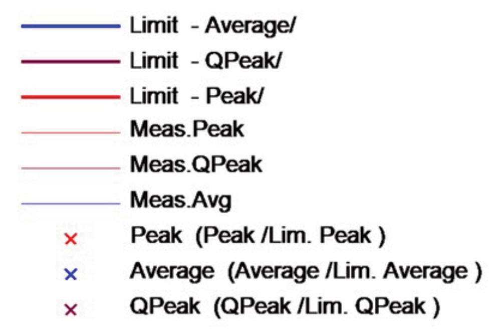
Conducted emission results legend list
Figure 9: Conducted emission results legend
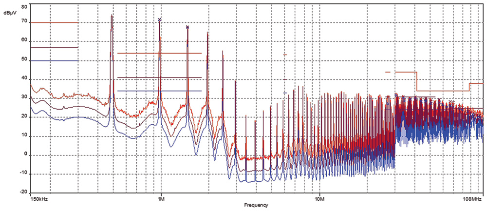
The test results on the battery line, in the frequency range of 150 kHz – 108 MHz, are shown in Figure 10 on page 54.
Conducted emission test results – BAT line – 150 kHz – 108 MHz graph
Figure 10: Conducted emission test results – BAT line – 150 kHz – 108 MHz
The conducted emissions plot of the Battery line, like the Monopole region of the RE test data, shows significant emissions at the switching frequency of the Buck regulator and the harmonics of this frequency. This measurement was taken with a 9 kHz resolution bandwidth from 150 kHz – 30 MHz and a 120 kHz resolution bandwidth from 30 MHz – 108 MHz. This shows the failure of all three limits at 978 kHz, and 1.4685 MHz. This also shows failures of the average and quasi-peak limits from ~25 MHz – ~100 MHz.

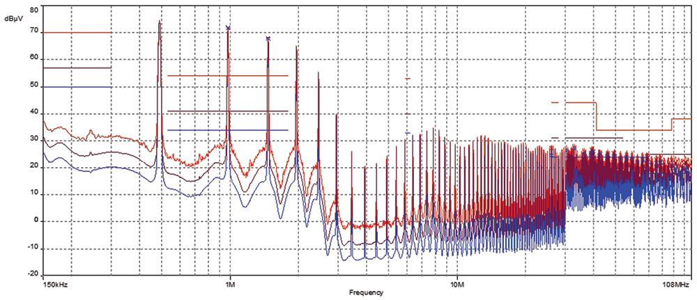
The test results on the ground line, in the frequency range of 150 kHz – 108 MHz, are shown in Figure 11 on page 54.

Conducted emission test results – GND line – 150 kHz – 108 MHz graph
Figure 11: Conducted emission test results – GND line – 150 kHz – 108 MHz
From this measurement of emissions from the GND line, it is seen that there is a similar amount of emissions coming from the Battery line and the GND line for this DUT. This measurement was taken with a 9 kHz resolution bandwidth from 150 kHz – 30 MHz and a 120 kHz resolution bandwidth from 30 MHz – 108 MHz. Like the Battery line measurements this shows failures of all three limits at 978 kHz, and 1.4685 MHz, and multiple failures of the average and quasi-peak limits from ~25 MHz – ~100 MHz.
4. CISPR 25 Conducted Emissions (Current Method) Test Results
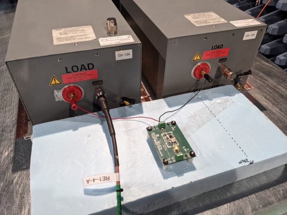
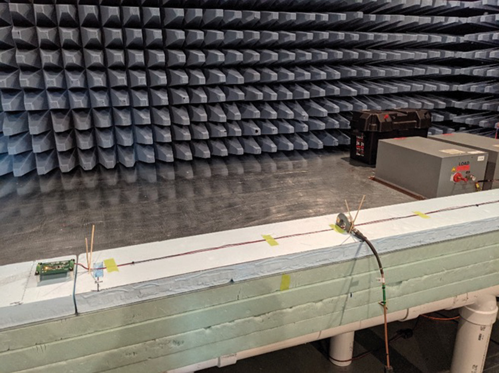
Figure 12 shows the current method conducted emissions test setup.
Conducted emission test setup (current method) room
Figure 12: Conducted emission test setup (current method)
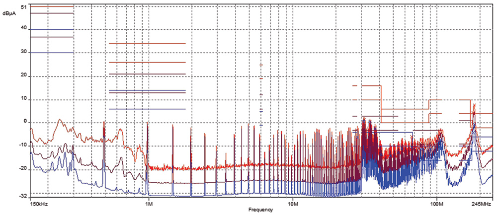
The test results, at 50 mm, in the frequency range of 150 kHz – 245 MHz are shown in Figure 13 on page 56. The measurement from 150 kHz – 30 MHz was taken with a 9 kHz resolution bandwidth, and the measurement from 30 MHz – 245 MHz was taken with a 120 kHz resolution bandwidth.
Conducted emission test results at 50 mm graph
Figure 13: Conducted emission test results at 50 mm
The conducted emissions measurement at 50 mm, shows significant broadband emissions from 25 MHz – 100 MHz, and at ~180 MHz.

These emissions are likely due to ringing in the switching waveform.

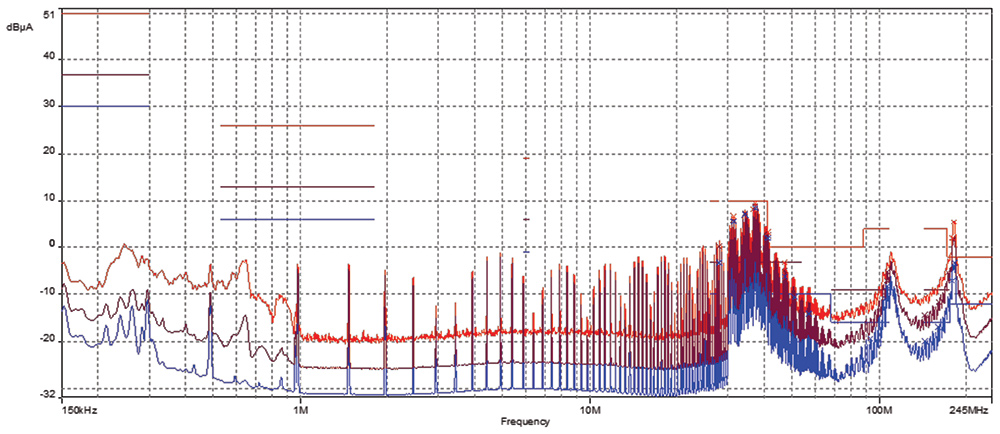
The test results, at 750 mm, in the frequency range of 150 kHz – 245 MHz are shown in Figure 14 on page 56. The measurement from 150 kHz – 30 MHz was taken with a 9 kHz resolution bandwidth, and the measurement from 30 MHz – 245 MHz was taken with a 120 kHz resolution bandwidth.

Conducted emission test results at 750 mm graph
Figure 14: Conducted emission test results at 750 mm
Like the 50 mm measurements, this measurement taken at 750 mm, shows significant broadband emissions from 25 MHz – 100 MHz, and at ~180 MHz. These emissions are likely due to ringing in the switching waveform.
5. Future Work
The next article will be devoted to the evaluation of EMC countermeasures to address the radiated and conducted emissions non-conformities. The article will address each test result and the impact of the optional EMC components.
References
  1. Adamczyk, B., Mee, S., Koeller, N, “Evaluation of EMC Emissions and Ground Techniques on 1- and 2-layer PCBs with Power Converters – Part 1: Top-Level Description of the Design Problem,” In Compliance Magazine, May 2021.
  2. Adamczyk, B., Mee, S., Koeller, N, “Evaluation of EMC Emissions and Ground Techniques on 1- and 2-layer PCBs with Power Converters – Part 2: DC/DC Converter Design with EMC Considerations,” In Compliance Magazine, June 2021.
Share this story:
Bogdan Adamczyk headshot
Dr. Bogdan Adamczyk is professor and director of the EMC Center at Grand Valley State University (http://www.gvsu.edu/emccenter) where he regularly teaches EMC certificate courses for industry. He is an iNARTE certified EMC Master Design Engineer. Prof. Adamczyk is the author of the textbook “Foundations of Electromagnetic Compatibility with Practical Applications” (Wiley, 2017) and the upcoming textbook “Principles of Electromagnetic Compatibility with Laboratory Exercises” (Wiley 2022). He can be reached at adamczyb@gvsu.edu.
Scott Mee smiling in a professional headshot
Scott Mee is a co-founder and owner at E3 Compliance which specializes in EMC & SIPI design, simulation, pre-compliance testing and diagnostics. He has published and presented numerous articles and papers on EMC. He is an iNARTE certified EMC Engineer and Master EMC Design Engineer. Scott participates in the industrial collaboration with GVSU at the EMC Center. He can be reached at scott@e3compliance.com.
Nick Koeller smiling in a professional headshot
Nick Koeller is an EMC Engineer at E3 Compliance which specializes in EMC & SIPI design, simulation, pre-compliance testing and diagnostics. He received his B.S.E in Electrical Engineering from Grand Valley State University and is currently pursuing his M.S.E in Electrical and Computer Engineering at GVSU. Nick participates in the industrial collaboration with GVSU at the EMC Center. He can be reached at nick@e3compliance.com.