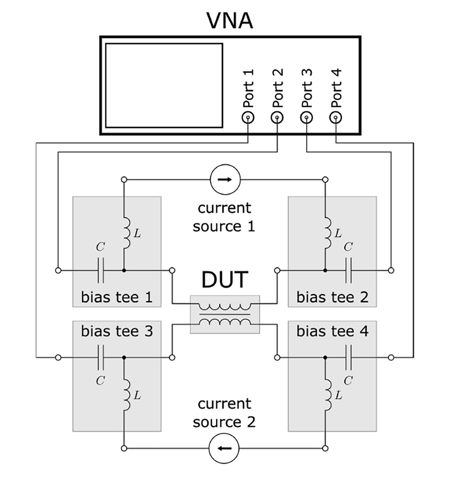
In many EMC applications, passive components need to be characterized to provide simulation models and physical insight into the dominant processes within these components. Passive filters consist of inductors and capacitors, some of which are 3- or 4-terminal devices, such as common-mode chokes. For small signals, these components can be considered linear with respect to voltage and current. However, in many applications, non-linear effects must be considered and characterized. This can be achieved with a time-domain large-signal approach or by linearization around certain bias points. Linearized characterization of potentially non-linear devices such as filter inductors or capacitors requires simultaneous excitation of the small-signal evaluation signal and the large-signal bias, which is current for inductors and voltage for capacitors. The most commonly used method relies on a vector network analyzer (VNA) and a bias network to apply the large signal bias.
For higher current or voltage levels, external bias tees must be used for VNA measurements. In particular, when these span a wide frequency range, here from 9 kHz to 500 mHz, they present the following challenges:
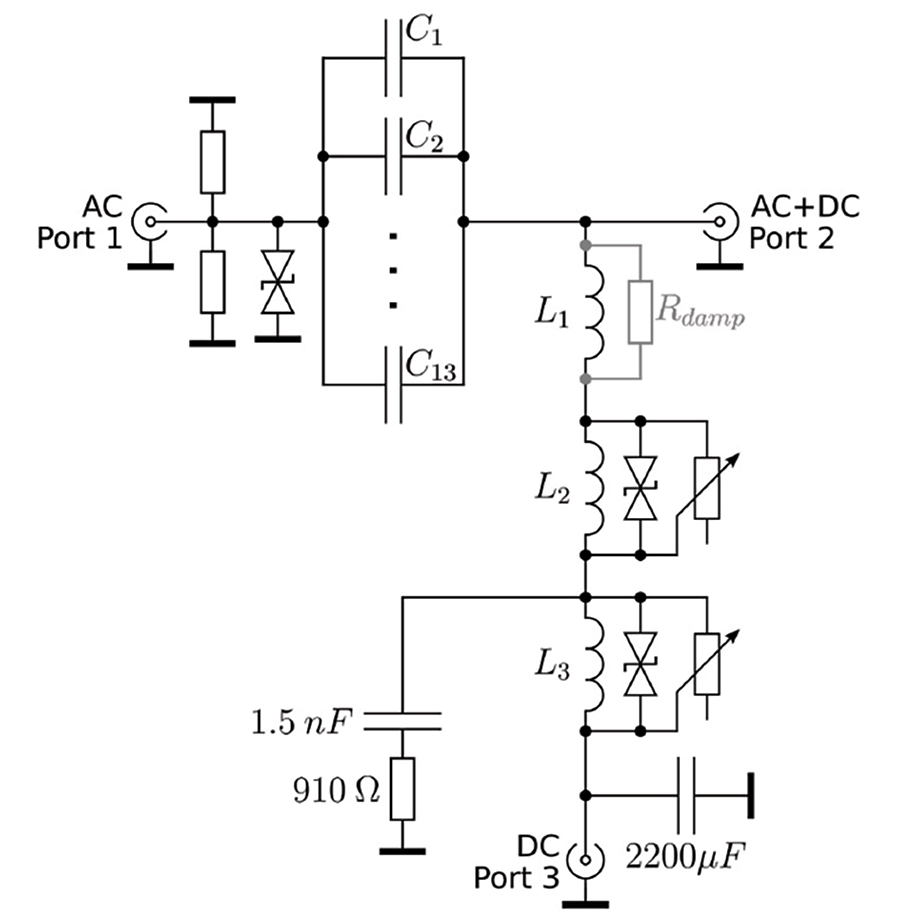
- The calibration plane is moved away from the VNA to a position after the bias tee. The basic assumption of the VNA calibration is time invariance. Any changes in the path from the VNA to the calibration plane that occur after the time of calibration are not corrected. Thermal expansion, such as in inductors, and saturation due to current or capacitance changes caused by the bias voltage can change the RF characteristics of the bias tee. Therefore, a thermally well-designed, highly linear bias tee is required.
- The bias tee will influence the RF path. It connects inductors for the DC feed to the RF path and it interrupts the RF path to block the DC voltage from reaching the VNA. In principle, the VNA calibration compensates for these effects. Even if these effects were completely time invariant, they would reduce the dynamic range of the test system if the calibration had to correct for large changes in the RF path through the bias tee. Thus, the RF path through the capacitor and the decoupling through the inductors requires a design that minimizes the effects on the RF path and thus does not require strong compensation by the calibration.
- The energy stored in mH inductors at 10 A current can endanger the VNA if the current path to the DUT is suddenly interrupted. Simply adding transient voltage suppression (TVS) diodes to the VNA is difficult because large diodes are required to handle the energy, but they have larger capacitances that will negatively impact the RF path. A distributed protection solution is therefore required.
For very low frequencies there are also interesting active solutions for bias tees [3], which again cannot be used for higher frequencies. However, the bias tee published in this paper is intended to be used primarily for the measurement of conducted electromagnetic emissions, for which a lower frequency limit of 9 kHz is quite adequate. A passive solution is therefore preferred.
Although some of the concepts described regarding the construction of the individual components are already known in the literature, to the best of the authors’ knowledge, there are no publications yet on such a composition for the construction of a bias tee. The particular advantage of this special form of bias tee is the possible use for small-signal characterization of power electronic components while maintaining high large-signal bias currents and voltages. By measuring the S-parameters of various power electronic components and measuring the changes due to bias over a large frequency range, valuable data can be easily obtained for modeling the behavior of these components under large signal bias. Measurements of this configuration show good results regarding important properties of the tee, like insertion loss, return loss and temperature behavior.

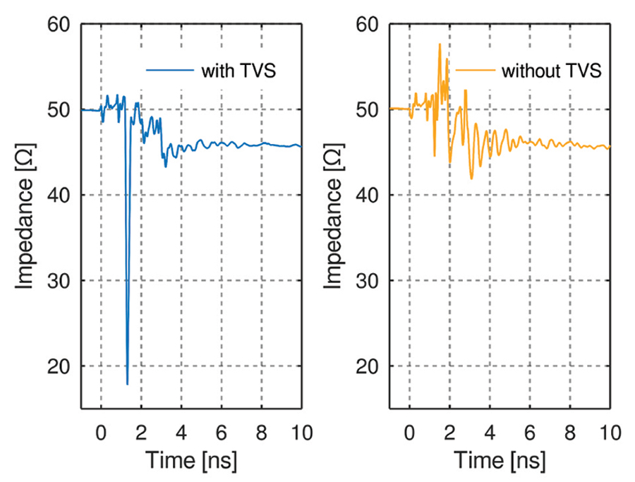
On a 1.6 mm FR-4 board a 3 mm wide trace leads to a 50 Ω characteristic impedance. To distribute the capacitances along the transmission line, thus to allow for a undisturbed TEM wave the capacitors are placed vertically, like it is shown in Figure 3. To match the trace width to the width of the capacitors two layers of 1.6 mm FR-4 are used creating a 6 mm wide microstrip line which allows placement of the capacitors without interrupting the RF path. Two carefully designed transitions guide the RF signal from the 3 mm wide trace to the 6 mm wide trace. Figure 4 shows the results of the designed microstrip line using a TDR measurement with a bandwidth of 14 GHz. It can be seen that the capacitive coupling of the TVS diodes used to protect the VNA, as discussed in the section “Protection Concept,” have an influence on the line. This influence can be counteracted by changing the diameter of the microstrip line at the point where the diodes are connected.
For the calculation of the necessary inductance values, a minimum impedance of 43 dBΩ (referred to 1 Ω) was aimed at. At the minimum frequency of 9 kHz this results in a necessary minimum inductance of about 2.5 mH. The needed bandwidth and current carrying capability poses several problems for the inductor design. High currents require thick wires which adds parasitics at high frequencies; not being able to use cores because of saturation effects increases the inductor size, which again is detrimental to the RF performance and the use of large value inductors increases the difficulty of over-voltage protection of the VNA in case the DUT current is suddenly interrupted. In addition, large coils have greater DC resistance and thus higher power dissipation, which leads to increased temperatures in the package (see the section “Temperature Behavior”).
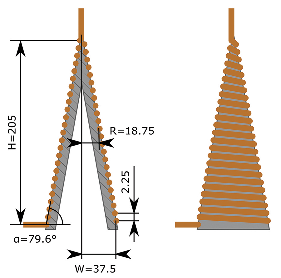
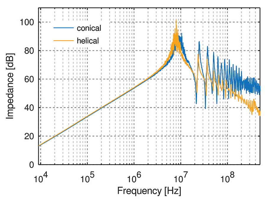
In order to optimize the behavior at high frequencies, a conical coil (L1), shown in Figure 5, was used. Following the design in [5] the conical inductor was connected to the 50 Ω microstrip line that holds the DC block. The advantages of a conical design over a cylindrical inductor can be seen in Figure 6. The conical shape improves the RF performance however, it offers less inductance compared to a cylindrical inductor having the same number of turns and length. Both inductors in the plot have the same inductance and do not use a magnetic core. Up to the resonance, no differences are visible. However, after the first resonance, the conical inductor shows a series of resonances maintaining in average higher impedance relative to its cylindrical partner. The distribution of these additional resonances depends on details of the winding, the wire diameter and the distance between the wires. The higher the frequency, the more important is the design of the tip of the conical inductor and its connection to the 50 Ω trace. According to [6] the inductance of the conical inductor can be derived from the inductances of related cylindrical and spiral inductors. The inductance of a spiral inductor in µH is given by Equation 1 where R is the mean radius of the inductor in mm, W is the radius difference on both cone ends in mm and N is the number of windings.
The inductance of a cylindrical (helical) inductor is given by Equation 2, where H is the coil height in mm and again R and N are the mean radius and the number of windings respectively.
Using LS and LH the inductance of a conical inductor can be obtained by Equation 3 where α is the angle of the conical inductor, being 0° for a totally flat inductor.

For this coil an inductance of about 63 µH is calculated with the geometrical values given in Figure 5. For achieving an inductance value of 2.5 mH the conical inductor would need to be more than three times as long, which is why two further coils of higher inductance (L2 = 0.27 mH and L3 = 2.2 mH) had to be connected in series behind it to reach the desired inductance value. The coils have a total DC resistance of 300 mΩ and thus dissipate 30 W at 10 A DC current.
- The anti-resonances may reach low impedance values. Those are placed in parallel to the 50 Ω trace, thus, at those frequencies the S12 of the RF path is diminished. This requires stronger correction during calibration.
- Even if they could be compensated by calibration, they must remain time invariant. Small geometrical changes, e.g., thermally induced may move the resonances. The higher the Q-factor is, the stronger small changes will impact the impedance.
- The inductors will warm up to 60 °C at 10 A current. This increases the wire resistance which increase damping. If the calibration would be based on high Q resonance even this small change may lead to an inaccurate correction during measurements by the stored calibration values.
Thus, it is advisable to introduce losses that dampen the resonances. This will reduce the impedance at resonances and increase the impedance at anti-resonances. Of the several available damping methods, electrically lossy material placed near the conical inductor was used for the first stage inductor, represented by Rdamp in Figure 2. Magnetically lossy material would pose the risk of introducing non-linear behavior due to the large DC current. Placing a resistor across the conical inductor would add parasitic capacitance to the connection point at the DC block on the RF path. The disadvantage of the electrically lossy material is its blocking effect on the cooling of the coil.
For the other inductors adjustable resistors have been placed in parallel to allow for a smooth impedance behavior which leads to a smooth loss characteristic show in Figure 8.
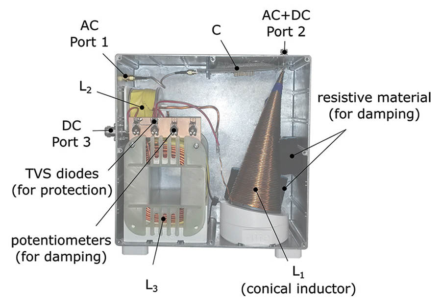
Without protection, a sudden interruption of current flow through the DUT, e.g., a solder joint breaks, will dissipate the stored energy into the VNA (RIP). Protective devices such as transient voltage suppressor (TVS) diodes are well suited to protect the VNA. If they are placed directly in the RF path, their capacitance needs to be kept small to avoid further disturbances on the RF path. However, those diodes cannot handle the energy. The problem is resolved by distributing diodes across the inductors. The high value inductors store most of the energy, but their electrical function is limited to lower frequencies, thus TVS having larger capacitance of about 100 pF can be used [7]. No TVS is placed across the conical inductor, instead 2.5 pF TVS are placed on the RF path [8].
A second protection problem arises from the 1.1 J stored in the DC block capacitors. If the DUT is suddenly shorted to GND the 8.8 µF charged at 500 V would be discharged into the VNA (RIP). The low capacitance diodes placed to protect against the energy in the conical inductor cannot handle the energy. A second level protection is needed. This is realized by placing polymer based snap back devices from the RF path to GND [9]. These devices offer very low capacitance < 0.05 pF, a fast turn on of 0.1 ns. After internal breakdown within the component, they clamp at about 25 V DC. The amount of energy in the DC block capacitor can destroy them and the TVS devices, but they protect the VNA in case of a short circuit.
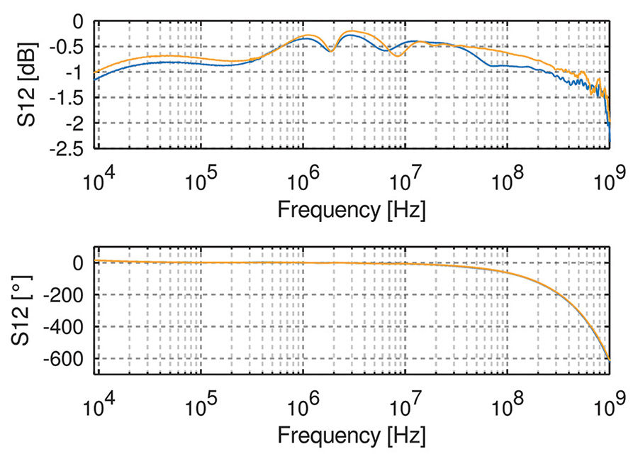
To verify the linear behavior the S-parameters of two identically built bias tees have been measured. Because of the well-defined impedance due to the large capacitor at the DC port, port 3 can be left open during calibration. In Figure 8 an insertion loss measurement of the two bias tees is depicted, which shows very satisfying results from 9 kHz up to a frequency of about 500 mHz with an insertion loss of less than 1 dB and an insertion flatness of about 0.5 dB. Above 500 mHz, the insertion loss increases to 2 dB at 1 GHz, largely due to the high frequency characteristics of the conical inductor. Measurements using conical coils with thinner wire showed better properties here but cannot pass the DC current. It can also be seen from the return loss measurement in Figure 9, that even though the two shown bias tees are built identically, their return loss differs quite significantly. This is the effect of slightly different coils and potentiometer settings. In general, one could create an S-parameter set for each bias tee and use this for de-embedding. Even though this procedure would result in better measurement performance, one would need the de-embedding profiles for each individual tee and must never interchange the bias tees for each measurement. Instead, a self-made calibration kit with previously measured de-embedding parameters was used. Two bias tees and the self-made calibration kit (TOSM) was used for calibration, which works regardless of the arrangement of the bias tees. For the final measurement, shown in Figure 1 a four-port calibration has to be done. In general, all calibration methods can run into the same limitations, which are small remaining non-linearities or mechanical changes due to heat or mechanical instability.
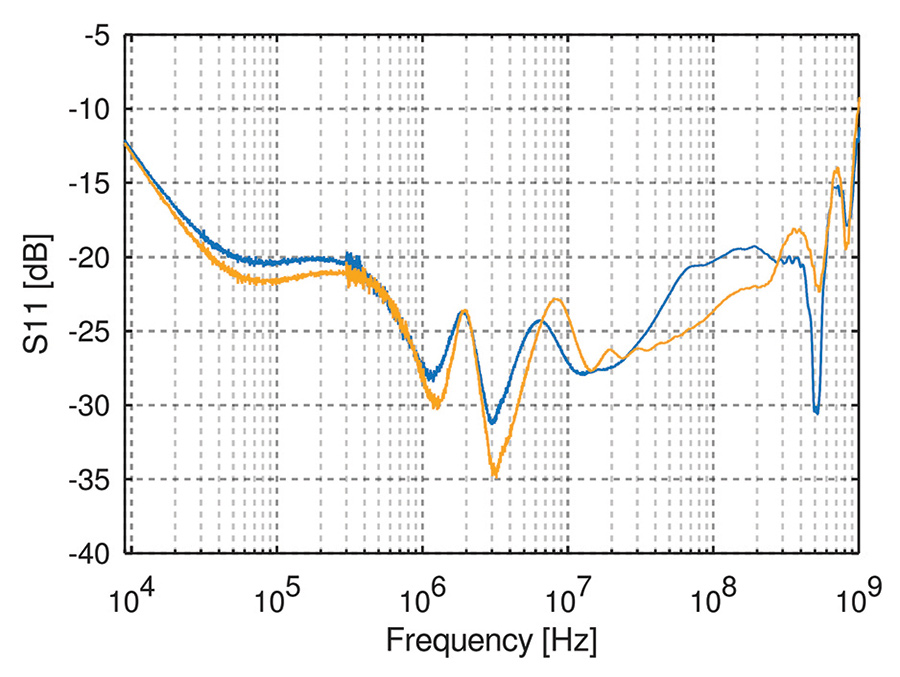
Figure 10 shows an S12 measurement of two bias tees connected in series at different DC bias currents. It can be seen that the DC bias current causes practically no difference in the behavior of the tees up to 25A.
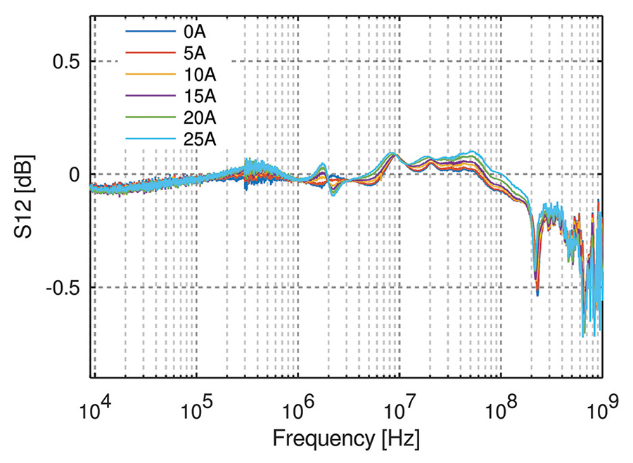
Figure 10: Insertion loss of two bias tees in series
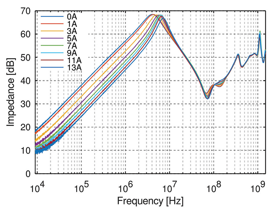
Figure 11 shows a test measurement of an inductor [10] at different DC bias currents between 0 A and 13 A. Saturation effects due to the DC bias current can be observed in the lower frequency range by a shift towards the right. At higher frequencies not much changes due to the bias current, since the permeability of the material has reduced to a level at which the flux cannot reach saturation levels.
- T. Stratil, P. Koudelka, J. Jankovych, V. Vasinek, R. Martinek, and T. Pavelek, “Broadband over visible light: High power wideband bias- t solution,” 2016 10th International Symposium on Communication Systems, Networks and Digital Signal Processing (CSNDSP), 2016, pp. 1–5.
- V. Major, J. Bacˇmaga, R. Gillon, and A. Baric´, “Design and characterization of bias tee used for s-parameter characterization of power inductors,” 2019 42nd International Convention on Information and Communication Technology, Electronics and Microelectronics (MIPRO), 2019, pp. 82–86.
- A. Nalli, A. Raffo, G. Avolio, V. Vadala`, G. Bosi, D. M. M. . Schreurs, and G. Vannini, “Extremely low-frequency measurements using an active bias tee,” 2013 IEEE MTT-S International Microwave Symposium Digest (MTT), 2013, pp. 1–4.
- Multilayer Ceramic Capacitors, NTS Series / NTF Series, United Chemi-Con, cAT. No. E1002X Ver.4. [Online]. Available: https://www.mouser.com/datasheet/2/420/ce-ntsntf-e-2018-1511727.pdf
- J. A. Nguyen and A. Gundavajhala, “Ultra broadband inductor assembly,” US Patent 7,142,086 B2, 2004. https://patents.google.com/patent/US7142086B2/en
- R. Linhart, V. Georgiev, and J. Kopal, “Broadband bias networks for pulse signal RF amplifiers,” 2015 International Conference on Applied Electronics (AE), 2015, pp. 153–156.
- “Surface Mount TRANSZORB® Transient Voltage Suppressors,” Vishay, 2013, Document number: 8839. [Online]. Available: https://docs.rs-online.com/1716/0900766b81410a00.pdf
- ”TVS Diode Arrays (SPA® Diodes),” Littelfuse, 2017. [Online]. Available: https://docs.rs-online.com/0a65/0900766b81622fb6.pdf
- “TVS Diode Series,” Bourns, 2019. [Online]. Available: https://www.mouser.at/datasheet/2/54/cdsod323-txxlc-777077.pdf
- “Differential Mode Choke Coils(RADIAL),” TDK, 2006. [Online]. Available: https://shop.griederbauteile.ch/en/info/h/HIN.pdf