EMC concepts explained
Evaluation of PCB Design Options on Analog Signal RF Immunity using a Multilayer PCB
Part 3: Conducted Immunity Testing
T

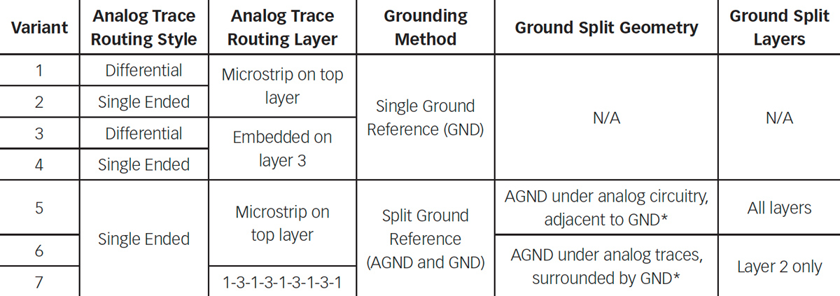
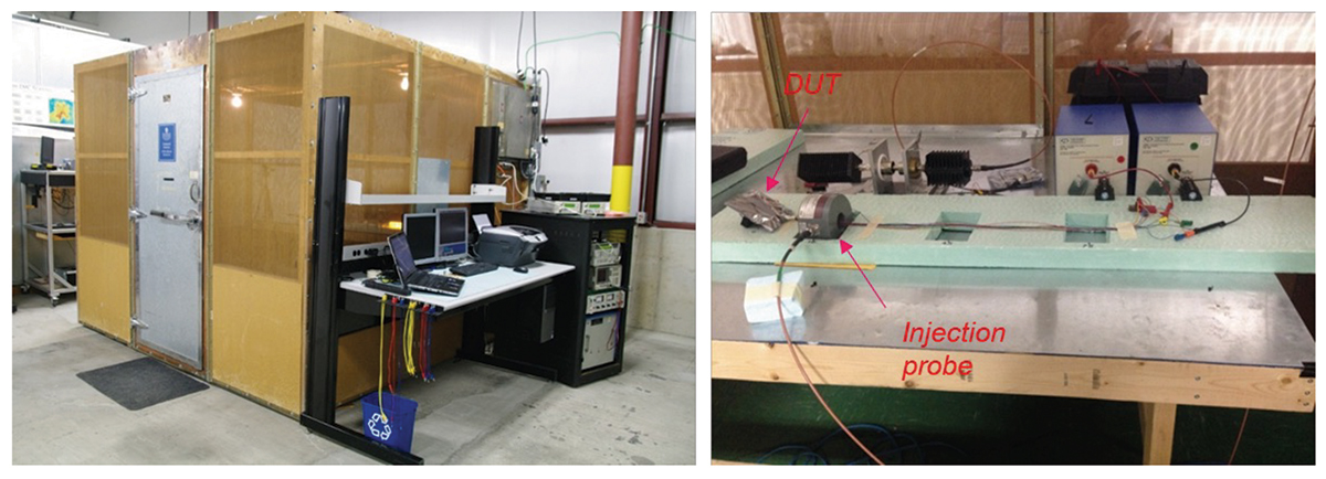
his month’s column is the last of three parts devoted to designing, testing, and EMC immunity evaluation of multilayer PCBs containing analog circuitry. The first article presented a top-level block diagram description of the design problem under research [1,2]. The second article discussed the radiated immunity results [3]. This article is devoted to the conducted immunity testing according to the ISO11452-4 Bulk Current Injection from 1 MHz – 400 MHz up to severity level 4. As a reminder, two analog measurements are present on the PCB. The first analog measurement captures analog temperature values from an NTC thermocouple at the end of a short harness. The second analog measurement captures the analog voltage of 12 volts connected at the banana jack terminals of the PCB. Both sets of values are processed by the microcontroller and reported to the test engineer outside the chamber via UART and fiber optic communications for isolation. However, for the purposes of this article, only analog temperature measurements are presented and discussed.

1. PCB Variants and Tests Configurations
In this study, there are seven design variants that all contain a similar schematic but implement different PCB layout techniques (see [2] for the details). The design variants are described in Table 1.
Design variants
Table 1: Design variants
Table 2 shows the test configurations used during the testing of the selected variants.
Description of test configurations
Table 2: Description of test configurations
The measurement setup for conducted immunity is shown in Figure 1 (see [4] for details).
2. Immunity Testing Results – Configuration A
Variant 1 and Variant 2 test results are shown in Figure 2.
ISO11452-4 measurement setup
Figure 1: ISO11452-4 measurement setup
Configuration A: Variant 1 vs. Variant 2
Figure 2: Configuration A: Variant 1 vs. Variant 2
Observations: Variant 1 tested in Configuration A exhibited anomalies (with exception of 1 to 2 MHz and 5 to 9 MHz) with the analog temperature readings. Variant 2 tested in Configuration A exhibited anomalies (with exception of 1 to 4 MHz) with the analog temperature readings. Compared to Variant 1, Variant 2 performed worse, especially above 9Mhz. This demonstrates that differential routing provided some benefit.

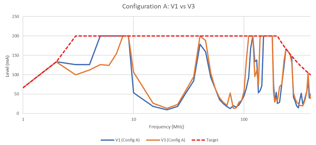
Next, Variant 3 was tested and the results were compared to those of Variant 1. The comparison is shown in Figure 3 on page 44.

Observations: Variant 1 performed better than Variant 3 at lower frequencies (2 to 7 MHz) and slightly better at higher frequencies. Beyond 10 MHz there aren’t significant differences between the two variants. This demonstrates that burying differentially routed traces beneath the ground plane on layer 2 did not provide an overall benefit above 7 MHz.

Next, Variant 4 was tested and the results were compared to those of Variant 2. The comparison is shown in Figure 4.

Configuration A: Variant 1 vs. Variant 3
Figure 3: Configuration A: Variant 1 vs. Variant 3
Configuration A: Variant 1 vs. Variant 3
Figure 4: Configuration A: Variant 2 vs. Variant 4
Observations: Variant 4 performed better than Variant 2 from 1 MHz to 9 MHz and from 120 MHz to 200 MHz. This demonstrates that burying the single ended traces on layer 3 beneath the ground plane on layer 2 provides an improvement in immunity performance in the respective frequency ranges.

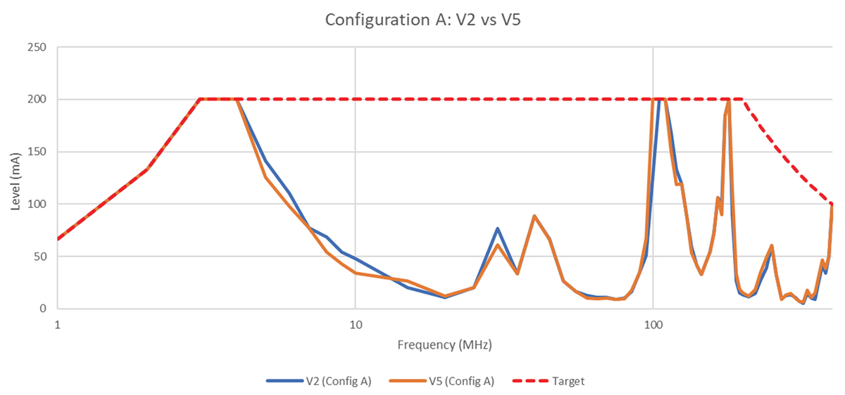
Next, Variant 5 was tested, and the results were compared to those of Variant 2. The comparison is shown in Figure 5.

Observations: Variant 5 performed similarly to Variant 2 across the entire spectrum. This demonstrates that splitting the grounds (GND and AGND) has a negligible impact on the conducted immunity performance. This is likely due to the fact that while there is a split between the two references, they both allow for a continuous reference return adjacent to the analog trace routes to provide a low inductance RF return path.

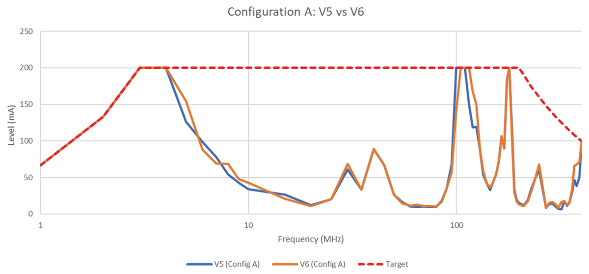
Next, Variant 6 was tested and the results were compared to those of Variant 5. The comparison is shown in Figure 6.

Configuration A: Variant 2 vs. Variant 5
Figure 5: Configuration A: Variant 2 vs. Variant 5
Configuration A: Variant 5 vs. Variant 6
Figure 6: Configuration A: Variant 5 vs. Variant 6
Observations: Variant 6 performed similarly to Variant 5. This demonstrates that splitting the grounds (GND and AGND) has a negligible impact on the conducted immunity performance. This is likely due to the fact that while there is a split between the two references, they both allow for a continuous reference return adjacent to the analog trace routes to provide a low inductance RF return path.

Next, Variant 7 was tested and the results were compared to those of Variant 6. The comparison is shown in Figure 7.

Configuration A: Variant 6 vs. Variant 7
Figure 7: Configuration A: Variant 6 vs. Variant 7
Observations: Variant 7 performed almost the same as Variant 6. This came as a surprise since Variant 7 has the analog nets alternating between layers 1 and 3 multiple times. One would assume that by routing the analog traces this way they would become more vulnerable to conducted immunity disturbances, however the data shows very little impact (positive or negative).
3. Immunity Testing Results – Configuration B
The three variants which exhibited the weakest RF immunity performance in Configuration A were re-tested in the same frequency range. For Configuration B, a conductive enclosure was added with non-conductive standoffs (ungrounded shielding). The weakest RF immunity was exhibited by the Variants 1, 5, and 6.

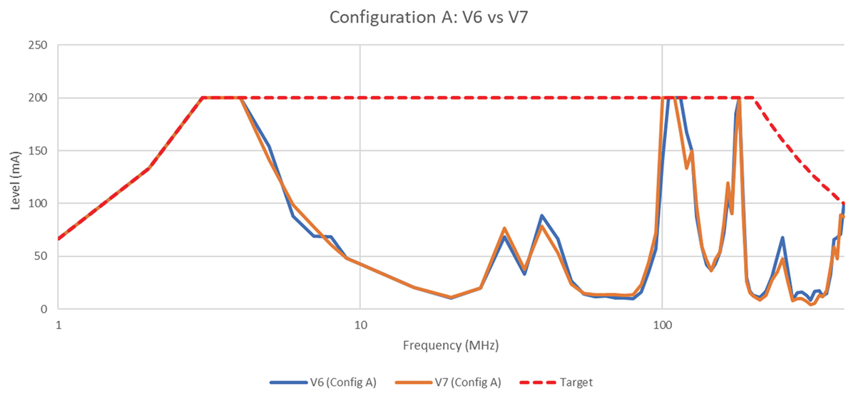
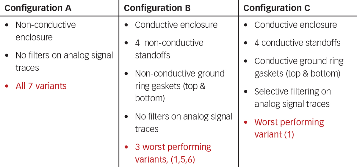
Figure 8 compares the test results for Variant 1, Configuration A vs. B.

Observations: Variant 1 in Configuration A generally outperforms Configuration B up to 9 MHz and beyond 90 MHz. Between 9 MHz and 90 MHz, Configuration B shows a benefit. Based on the data, an ungrounded shielded enclosure provides benefit in a limited frequency range when routing the analog trace differentially on the top side.

Figure 9 compares the test results for Variant 5, Configuration A vs. B.

Variant 1 – Configuration A vs. B
Figure 8: Variant 1 – Configuration A vs. B
Variant 5 – Configuration A vs. B
Figure 9: Variant 5 – Configuration A vs. B
Observations: Variant 5 in Configuration B performed similarly to Configuration A with the exception of 100 MHz – 130 MHz range and at 190 MHz where Configuration A did better than Configuration B. There are no benefits of Configuration B over Configuration A and Configuration B exhibited two areas of degradation at the frequencies mentioned. This is most likely due to the split ground strategy and lack of conductive standoffs that introduce a discontinuity in the shielding effectiveness from the enclosure and PCB reference plane areas.

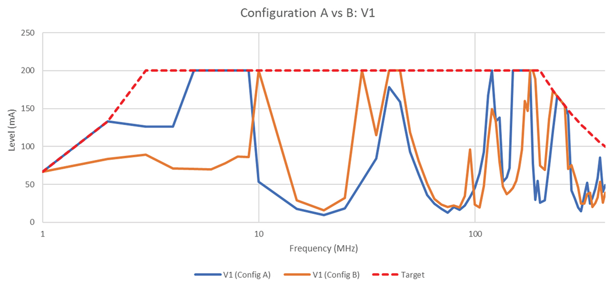
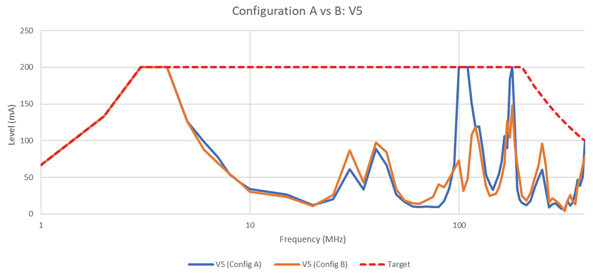
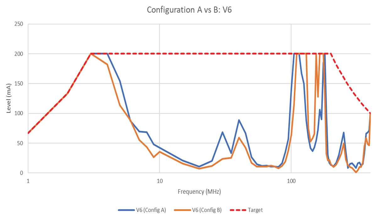
Figure 10 compares the test results for Variant 6, Configuration A vs. B.

Observations: Variant 6 in Configuration A performed better than Configuration B with the exception of the frequency range 110 MHz – 180 MHz where the ungrounded shielding provides some benefit. However, there are inconsistent benefits overall of introducing an ungrounded conductive enclosure (Configuration B). In Variant 6, the analog traces are routed on the top layer with PCB GND surround and a separate Analog GND is beneath on Layer 2. All other layers are PCB GND. These layout design features minimize the ungrounded shielded enclosure’s impact on the conducted immunity performance.

4. Immunity Testing Results – Configuration C
Finally, the worst-performing variant from Configuration B (Variant 1) was re-tested in the same frequency range according to Configuration C (conductive standoffs, conductive gasket, selective filtering components on analog lines). Figure 11 compares the test results for Variant 1, Configuration A vs. C.
Variant 6 – Configuration A vs. B
Figure 10: Variant 6 – Configuration A vs. B
Variant 1 – Configuration A vs. C
Figure 11: Variant 1 – Configuration A vs. C
Observations: Variant 1 in Configuration C performed dramatically better than Configuration A over a wide band of frequencies from 9 MHz to 400 MHz. Improvements were made due to the shielded enclosure, conductive standoffs, conductive gaskets, and selective filtering components on the analog lines. Since Configuration B (shielded enclosure, non-conductive standoffs) didn’t provide as much benefit as Configuration C, the added conductive gaskets, conductive standoffs, and component filtering likely provided the most benefit.
Summary
In summary, there are conducted immunity benefits to burying analog lines on internal layers and keeping a consistent reference alongside and/or beneath the analog traces. Additional benefits can be achieved by filtering the analog signals and adding a shielded enclosure with good conductive seals and bonding to PCB GND reference planes. Findings from this study show that some of the disturbance from the bulk current injection probe radiates directly to the PCB and the conducted disturbance on the harness lines.
References
  1. Baatar, B., Costantino, C., Morey, R., Muldowney, C., EMC PCB Design Study, GVSU senior project sponsored by E3 Compliance, LLC.
  2. Adamczyk, B., Mee, S., Baatar, B., “Evaluation of PCB Design Options using a Multilayer PCB – Part 1: Top-Level Description of the Design Problem,” In Compliance Magazine, May 2022.
  3. Adamczyk, B., Mee, S., Baatar, B., “Evaluation of PCB Design Options using a Multilayer PCB – Part 2: Radiated Immunity Results,” In Compliance Magazine, June 2022.
  4. Adamczyk, B., Mee, S., “Bulk Current Injection (BCI) – Substitution Method and Closed-Loop Method with Power Limitation,” In Compliance Magazine, June 2018.
Share this story:
Bogdan Adamczyk headshot
Dr. Bogdan Adamczyk is professor and director of the EMC Center at Grand Valley State University (http://www.gvsu.edu/emccenter) where he regularly teaches EMC certificate courses for industry. He is an iNARTE certified EMC Master Design Engineer. Prof. Adamczyk is the author of the textbook “Foundations of Electromagnetic Compatibility with Practical Applications” (Wiley, 2017) and the upcoming textbook “Principles of Electromagnetic Compatibility with Laboratory Exercises” (Wiley 2022). He can be reached at adamczyb@gvsu.edu.
Scott Mee
Scott Mee is a co-founder and owner at E3 Compliance which specializes in EMC & SIPI design, simulation, pre-compliance testing and diagnostics. He has published and presented numerous articles and papers on EMC. He is an iNARTE certified EMC Engineer and Master EMC Design Engineer. Scott participates in the industrial collaboration with GVSU at the EMC Center. He can be reached at scott@e3compliance.com.
Bilguun Baatar
Bilguun Baatar is an electrical engineer specializing in EMC design and testing. He graduated from Grand Valley State University with a BSE in Electrical Engineering and his focus is on EMC pre-compliance testing and expanding the understanding of EMC concepts/procedures. He can be reached at bilguun.baatar@e3compliance.com.