

s semiconductor technologies advance toward smaller CMOS nodes, heterogeneous integration, and ultra-high-speed I/O interfaces, the design of electrostatic discharge (ESD) protection has become significantly more challenging. Traditional rule-based and empirical methods are no longer adequate for ensuring robustness across increasingly complex, multi‑domain, and multi-technology systems.
To address these challenges, the ESD Association Technology Roadmap [1] outlines a forward‑looking strategy built on three major pillars:
- Advanced Electronic Design Automation (EDA) tools
- Machine Learning (ML) for ESD data analytics
- SPICEbased modeling for ESD design and verification
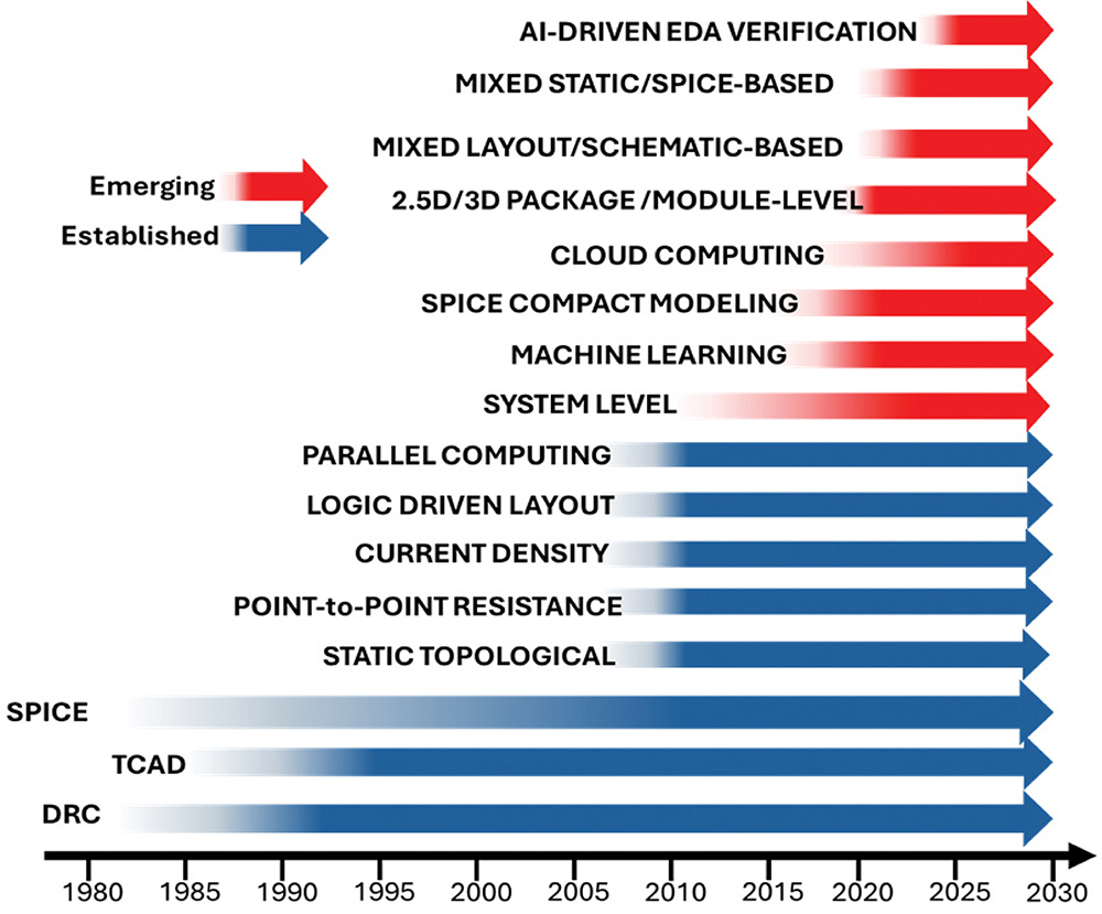
To address scalability, EDA vendors are incorporating:
- Parallelized execution engines
- Cloud-based distributed computing
- Hardware acceleration (xPU architecture)
The roadmap emphasizes:
- Development of common specification syntax
- Seamless interoperability between IC and package EDA tools
- Unified verification environments spanning schematic, layout, and module abstraction levels
Emerging flows integrate:
- SPICE simulations within topology-based EDA checks
- Automated generation of SPICE netlists from topology-based EDA checks
- Dynamic evaluation of power-domain crossings and complex protection scenarios
- Automated rule coding assistance
- Intelligent classification of violations
- Suggestion engines for corrective actions
Machine learning is proposed to increase efficiency and reduce evaluation uncertainty.
- Detect failure signatures at early symptom onset
- Avoid redundant stress testing for previously identified root causes
- Recognize recurring parameter shifts and correlate them to known degradation mechanisms.
- Identify likely root causes from waveform or parametric signatures
- Accelerate correlation between device behavior and protection topology
- Reduce iteration cycles in protection optimization.
However, practical deployment requires:
- Reduced training computational cost
- Memory-efficient implementations
- CAD tool integration compatibility
The primary barrier has been the absence of accurate ESD-capable compact models.
- High-current and high-voltage regimes
- Snapback in SCRs, BJTs, and MOSFETs
- Voltage overshoot
- Pulse rise-time dependence of trigger voltage (Vt1)
- Conductivity modulation
- Self-heating effects
- Forward/reverse diode recovery
- Release of the ASM-ESD diode model (2023; updated 2025)
- Initiation of an industry-standard ESD MOSFET model
- Hybrid architecture: regular FET model + Verilog-A ESD wrapper
By 2030, multiple standard ESD compact models will be based on ESD verification integrated into broader design flows.
This convergence represents a fundamental shift from rule-centric to model-centric ESD design methodology.
- Scalable, layout‑aware EDA verification
- AI‑assisted violation analysis
- Machine‑learning-driven data interpretation
- Standardized, ESD-capable SPICE models
The author extends appreciation to the following WG18 members for their review, guidance, and subject‑matter insights:
- Eleonora Gevinti, STMicroelectronics
- Nicolas Richaud, Intel
- Matthew Hogan, Siemens
- Scott Ruth, AMD
- Mirko Scholz, Infineon Technologies
- Michael Stockinger, NXP Semiconductors
- Paul Zhou, Analog Devices
- ESD Association Technology Roadmap, August 2025.

Dr. Michael G. Khazhinsky is a Principal ESD Engineer at Silicon Labs with advanced degrees in physics and engineering. He chairs ESDA Working Group 18 on EDA, has co‑authored over 60 papers, earned multiple best paper awards, and holds 18 patents. He currently serves as Vice President of the ESD Association.