Time and Frequency Domain Measurements
his article is the first of a two-article series devoted to the topic of crosstalk between PCB traces. This topic was previously discussed in [1] and [2]. In [1], we used a first-generation PCB and concentrated on signal integrity or the time domain measurements. In [2], we used a redesigned PCB to show the time domain impact of the guard trace on crosstalk. This two-article series presents measurements taken with a third-generation PCB. These measurements were taken both in the time domain using an oscilloscope and in the frequency domain using a near-field H probe. In Part 1 of the series, we vary circuit topology, i.e., the distance between traces and the distance to the ground plane. Both the time domain and frequency domain measurements show (for the topologies tested) that bringing the ground plane closer to the signal plane has a larger impact on reducing crosstalk than increasing the distance between traces. In Part 2 (to appear in the next issue), we investigate the impact of guard trace on crosstalk reduction, both in time and frequency domains.

Two PCB traces in a microstrip configuration are separated from each other by a distance s and from the ground plane (which is a return conductor for both) by a distance d. The first trace (generator conductor) is driven by a time-varying voltage source VS with the impedance RS and terminated by a load resistor RL. The second trace (receptor conductor) is terminated by the load resistors RNE and RFE on the near end and the far end, respectively.
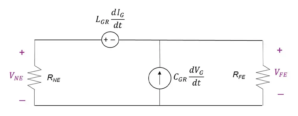
Superposition of the inductive and capacitive coupling mechanisms results in the receptor circuit shown in Figure 2, where LGR and CGR represent the mutual inductance and mutual capacitance, respectively, between the generator and receptor circuits (this model is valid for electrically short structures).


- If VS = const, then VNE(t) = 0 and VFE(t) = 0.
- A faster rise or fall time, dVS /dt, results in larger values of VNE(t) and VFE(t).
- On the rising edge of VS(t), dVS /dt > 0, and both the inductively and capacitively induced near-end voltages are positive; VNE,ind > 0, VNE,cap > 0.
- On the rising edge of VS(t), the inductively induced far-end voltage is negative, VFE,ind < 0, while the capacitively induced far-end voltage is positive, VFE,cap > 0.

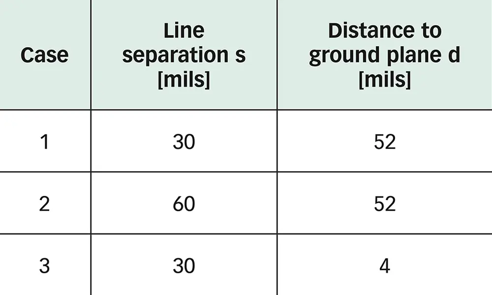

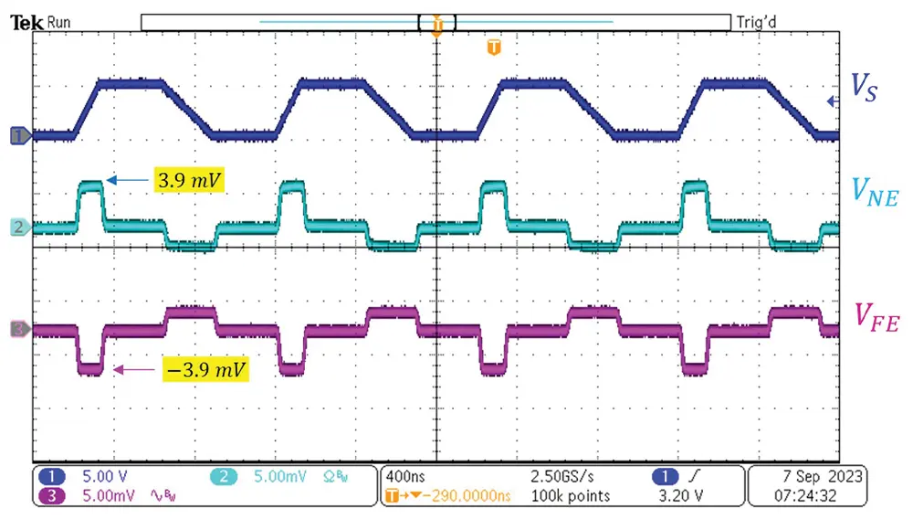


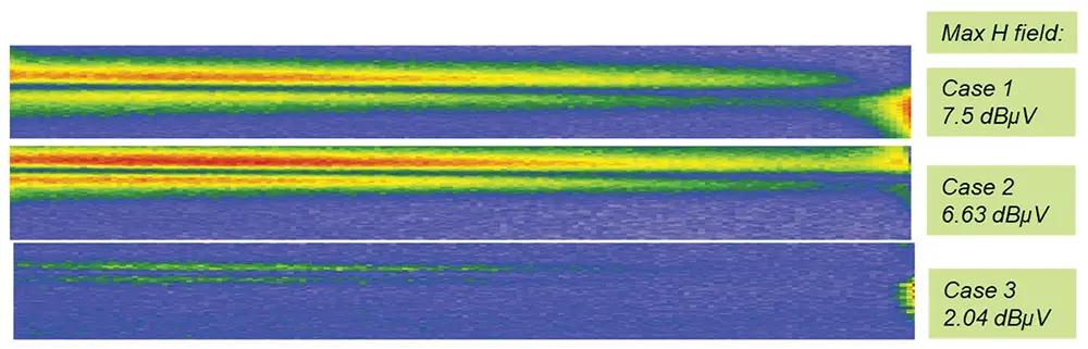
Figure 8 shows the measurement results at 9 MHz, while Figure 9 shows the results at 49 MHz. These measurements are summarized in Table 2.


- Bogdan Adamczyk and Jim Teune, “Crosstalk Reduction between PCB Traces,” In Compliance Magazine, March 2017.
- Bogdan Adamczyk, Principles of Electromagnetic Compatibility: Laboratory Exercises and Lectures, Wiley, 2024.
- Howard Johnson and Martin Graham, High‑Speed Digital Design – A Handbook of Black Magic, Prentice Hall, 1993.


Mathew Yerian-French is an electrical engineer specializing in EMC design and diagnostic testing. He received his B.S.E in Electrical Engineering from Grand Valley State University. He focuses on preventing EMC issues through design reviews and early EMC pre‑compliance testing and diagnostics. Mat participates in the industrial collaboration with GVSU at the EMC Center. He can be reached at mathew.french@e3compliance.com.