ue to the proliferation of wireless applications ranging from cellular and automobile communication systems to the Internet of Things, RF switching and tuning solutions continue to provide challenges for both device and system-level ESD protection. Most of the RF switching that is needed is built in the silicon-on-insulator (SOI) process technology, as shown in Figure 1. Thin-film SOI provides the substrate that enables both the high RF performance and the transistor isolation needed for high-power RF signal processing. One of the intrinsic advantages of the SOI RF switch is the self-protection it can provide for device-level ESD threats [1]. Furthermore, when properly co-designed with the system-level ESD protection, the SOI switch can contribute to the protection of the total antenna system.
Understanding this self-protection mechanism and then successfully modeling it is critical for the SOI switch circuit designer. The turn-on mechanism for the switch in an ESD event is actually the synergy of two mechanisms [2,3]. The large gate resistance (RG) and the gate capacitance (CGD) result in an RC time constant that is sufficiently large that, when the ESD pulse strikes the switch, the switch transistor gate couples up, turning the transistor array on. Assisted by this channel current and initiated by the avalanche breakdown at the transistor drain, the parasitic bipolar turns on, providing the secondary ESD protection mechanism. The TLP plot of the response of a single stack switch to the ESD pulse, as well as the dual protection mechanism, is shown in Figure 2. In Figure 2(a), the gate bias during the TLP testing was 1V.

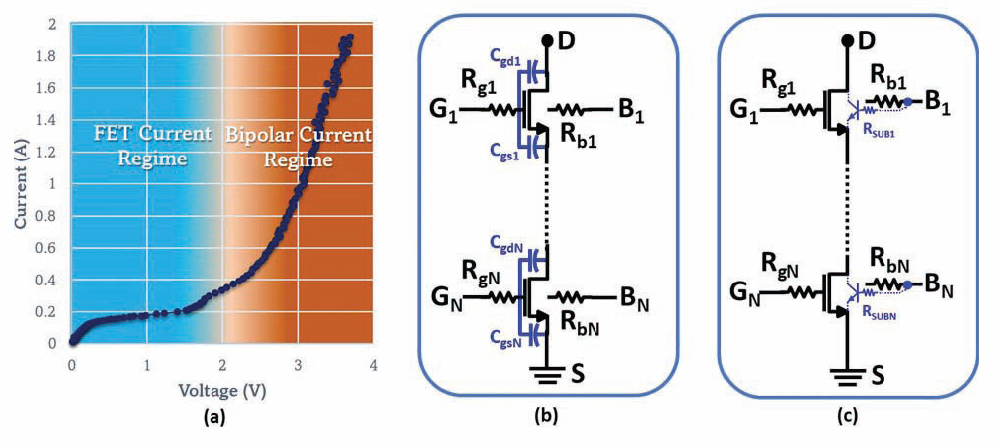
To address the deficiencies of the curve-fitting model, a behavioral model that comprehends the dual mechanism of the switch turn-on in an ESD event has been proposed [3,4]. Figure 3 graphically shows the behavioral model of the NMOS in a multiple-stack RF switch. This model contains two parts connected in parallel: the standard FET model for NMOS channel conduction and the ESD model for the parasitic bipolar turn-on. While this is an oversimplification of the behavior observed in Figure 2(a), the ESD model is considered an ideal switch in series with a resistor. The switch turns on at the parasitic bipolar trigger voltage (VTR) to shunt the ESD current with a fixed on-resistance (RON). The values of the two ESD model parameters can be extracted from the TLP measurement data of multiple-stack SOI RF switches.
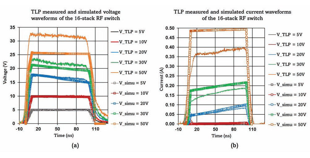
Figure 4 shows the time‑domain voltage and current waveforms of a 16-stack RF switch from the TLP measurement and the corresponding transient simulations for stress voltages of 5V to 50V. As is observed in Figure 4, the simulation and measurement match quite well for TLP voltages below 20 V. However, for stress voltages above 20V, the simulation and measured data begin to diverge. This divergence is due to the oversimplification of the ESD model for bipolar conduction. To model the ESD behavior more accurately in the high current regime, the simple turn-on of an ideal switch with a fixed on‑resistance would need to be replaced with the more complicated model of the turn-on of the NMOS parasitic bipolar transistor. This is one of the ongoing efforts in the refinement of the ESD modeling of the SOI switch response to the ESD event.

- A. Tombak, M. S. Carroll, D. C. Kerr, J.‑B. Pierres, and E. Spears, “Design of high-order switches for multimode applications on a silicon-on-insulator technology,” IEEE Transactions on Microwave Theory and Techniques., vol. 61, no. 10, pp. 3639-3649, October 2013.
- J. Liu, N. Carels, and N. Peachey, “Characterization and Analysis of RF Switches in SOI Technology for ESD Protection,” 2022 IEEE International Reliability Physics Symposium (IRPS), Dallas, TX, USA, 2022, pp. P13-1-P13-5.
- J. Liu and N. Peachey, “A Behavioral Model for ESD Self-Protection RF Switches in the SOI CMOS Technology,” 2022 International EOS/ESD Symposium on Design and System (IEDS), Chengdu, China, 2022, pp. 1-8.
- M. Di, A. Nath, M. Miao, X. X. Lu, L. Lin, and R. Gauthier, “Electrostatic Discharge Switch Simulation Enablement in RF SOI Technology,” 2021 IEEE International Symposium on the Physical and Failure Analysis of Integrated Circuits (IPFA), Singapore, 2021, pp. 1-5.