new version of Technical Report TR18.0-01-25 (TR18) on ESD Electronic Design Automation (EDA) Checks by the ESD Association’s Working Group 18 is about to be released. This article, divided into Part 1 and Part 2, provides guidelines for the EDA industry and the ESD design community for establishing a comprehensive ESD verification flow to address the ESD design challenges of modern ICs. Part 1 covered the concept of ESD checks throughout the IC Design Flow, including Schematic-based and Layout-based ESD checks. Part 2 covers Package-level and System-level checks, ESD Circuit simulation, and ESD TCAD simulation, completing the coverage of all ESD EDA checks described in the Technical Report.
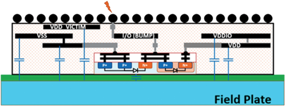
To ensure that the designed protection levels are maintained across all package options, the current state of package-level ESD verification involves several critical steps: extracting metadata of die pads and package pins, setting up EDA tools, defining ESD targets for each signal IO and supply pin, applying appropriate ESD rules on design, and verifying the integrity of the overall ESD protection network considering the additional RLC paths introduced by the package.
Advanced packaging technologies, such as 2.5D and 3D integrations, introduce additional challenges like differentiation between internal (die‑to-die) and external IOs, the huge number of die-to-die IOs to check, integration of chiplets from different process technologies/foundries, use of SI‑interposers and TSVs, and ESD risk associated with the final assembled package and the assembly process itself.
System-Level ESD Checks
If a failure occurs during a PCB-level ESD qualification, the following analysis methods can be used to diagnose the root cause: perform SEED analysis of the PCB path containing the failed IC component, perform scanning analysis by applying near-field electromagnetic interference pulses to failing areas of the PCB topology, or execute a full wave analysis on the failing PCB to identify the failing topology.
An HBM ESD source is typically modeled as an equivalent lumped circuit to produce the exponentially decaying current pulse (Figure 1a). A CDM ESD source can be similarly represented, or by an array of capacitors attached to the IC in a distributed manner to model the field coupling from the CDM tester (Figure 1b). A behavioral approach is also applicable, such as using a damped sinusoidal wave to simulate CDM current pulse.

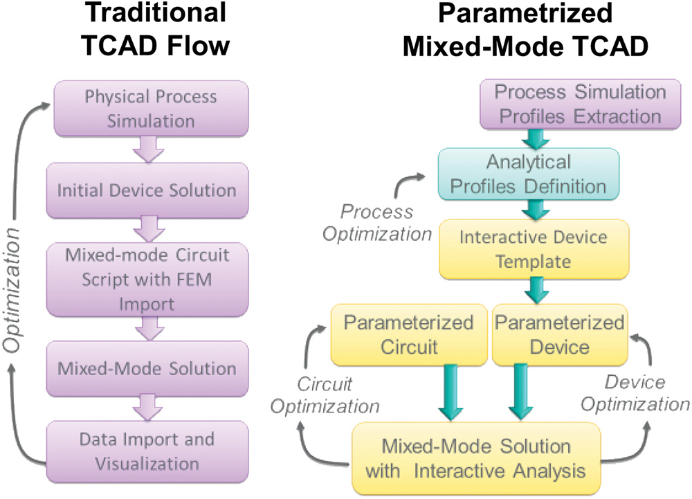
ESD TCAD Simulation
TCAD applications are effective at the technology and ESD IP development stages. One of the most important representations of a TCAD approach for EDA is mixed-mode simulation, which extends transient simulations’ capabilities from a single device structure to several devices within small circuits (Figure 2).