Hot Topics in ESD
Evolution of Charged Device Model ESD Target Requirements
Historical Background
CDM is an important model for ESD qualification. The well-known CDM refers to the discharge of an IC package to a grounded surface, whether from automatic handlers in a production area or from when placing IC packages in empty sockets. However, it is strange that during the early years of ESD focus, CDM had not been either addressed as a big threat in a more urgent manner or even if considered, was always a step-sister for the HBM focus. It is not that there was not much recognition of the potentially serious issues for CDM threat.

It was in 1974 that Thomas Speakman that first mentioned, “CDM is as important as HBM” [1]. Also, credit should be given to Bossard et al. for first reporting about triboelectrically charged pins [2]. Then during the mid-1980s, workers from British Telecom performed the first experiments on the field-induced CDM threat [3]. This was quickly followed by the work of Siemens, where they demonstrated evidence of DRAM devices failing due to uncontrolled CDM in a production area. These events motivated the serious work on a CDM simulator [4] and Field-Induced CDM test methods. Thereafter, the focus on CDM rapidly increased, and IC protection methods to counter CDM started to develop. The factory control methods for CDM were also established where additional steps of controlling insulators, avoiding hard discharges, and controlling changed boards and devices are more than safe for 500 V CDM and even for 250 V CDM [5].

Realistic CDM Targets
The requirements for CDM target levels initially were set from customers, with no manufacturing or customer data to support them; levels of 750 and 1000V became commonplace and with some customers, mandatory. As applications for IC devices started advancing and the high-speed IO pins became part of the microprocessor technology, the 500 V CDM became increasingly difficult to achieve in design. As these challenges for 500 V CDM started increasing, which also incidentally affected the perennial 2 kV HBM requirement, the Industry Council performed exhaustive studies of shipped devices to the field at various passing levels of HBM or CDM and found no correlation to field returns with rates of <1 DPM [5,6]. As a result, 1 kV for HBM and 250 V CDM were deemed safe for all practical design considerations. Manufacturing ESD control methods for CDM target levels for manufacturing/assembly areas were detailed in [5].
High-Speed IO Requirements and Challenges for CDM
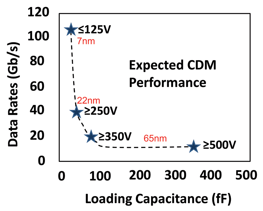
Starting around the late 1990s, the concern for CDM target level started becoming an issue as the higher speed IO applications increasingly could not meet the expected CDM levels. The problem came from the introduction of microprocessors that were built in very advanced silicon technologies, with their IO applications demanding high data rates. At the same time, these processors were packaged in large BGA packages to accommodate the high density of designs with numerous high-speed IO pins on the IC package. The combined effects place severe restrictions on the achievable CDM targets. That is, advanced scaled technologies lead to lower breakdown voltages for the transistors, and at the same time, larger IC package sizes lead to higher CDM peak current for the same CDM stress voltage. These BGA package sizes have since increased from about 1000 pins as the largest device during early 2000 to now approaching nearly 6000 pins in 2020. At 500 V CDM, the capacitance from these packages can develop enough charge in a CDM charging event to result in peak CDM discharge currents from 6 Amps to nearly 14 Amps. On the other hand, the loading capacitance from the I/O pin ESD devices has to be reduced to achieve high data rates, necessary for high-speed serial (HSS) link designs. With the ensuing requirements of smaller diode sizes that are more resistive, combined with lower oxide breakdown voltages in 22 nm and beyond, the CDM passing voltage level rapidly tends to decrease for even higher data rate designs. Eventually, for data rates approaching 224 Gb/s, the loading capacitance is limited to < 50fF, forcing expected CDM designs to meet only 125V. This overall effect is shown below in Figure 1 along with corresponding to the technology nodes for these respective data rates.
line graph showing achievable data rates
Figure 1: Achievable data rates versus loading capacitance from the ESD protection design as a function of advanced technology nodes in CMOS.
The Channing Roadmap
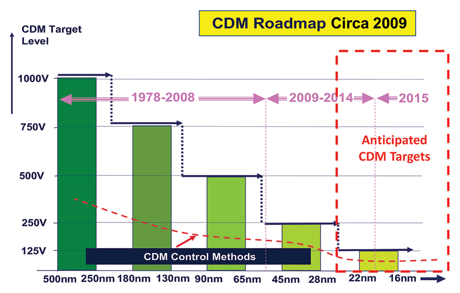
As presented so far, the roadmap for CDM has constantly changed based on demands for adjustments to accommodate high-speed IO performance, compounded by restrictive process technology limitations and the use of larger IC package devices. This gradual reduction in practical target levels for CDM can be understood first from Figure 2 and then followed by Figure 3 on page 35. Starting from the first specified CDM targets of 1000 V during 1990, the targets reduced to 500 V as technology advanced to 90 nm nodes (the late 1990s), and eventually, this was recommended to be reduced to 250 V starting at 45 nm nodes. This last step took coordinated studies from the Industry Council to prove that with the basic manufacturing ESD controls this 250V level is safe and can allow high-speed designs [5]. During the year 2009, the Council also anticipated that these levels may need to be reduced to 125 V starting at 22 nm and lower technologies, as also indicated in Figure 2.
chart showing projected CDM Roadmap during 2009
Figure 2: Projected CDM Roadmap during 2009.
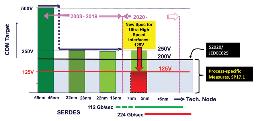
However, the reality of maintaining CDM sensitivity continued to be important even at 22 nm nodes, although the protections designs were beginning to face constrictions from lower breakdown voltages from the IO transistors. But this started changing around the year 2020 that ultra-high-speed interface designs at 5 nm and 7 nm FINFet technologies cannot meet 250 V CDM and that this has to be reduced to 125 V for these particular applications. This is indicated in Figure 3. To meet 112 Gb/Sec and higher, this lowering is mandatory, as indicated by the red arrow in Figure 3. But it must be mentioned that even at these advanced technology nodes, 250 V is still achievable for IOs known as General Purpose IO (or GPIO). That is, 125 V CDM is recommended only for ultra-high-speed interfaces. This is indicated in the update of [5], which is currently under preparation and will be released during 2021.
realistic CDM Roadmap as a function of immediate and future technology nodes
Figure 3: Realistic CDM Roadmap as a function of immediate and future technology nodes.
With the above-forecasted CDM target level reductions, it becomes very important to implement both improved manufacturing ESD control and ESD measurement methods as well as implement more reliable and accurate CDM measurement methods. There has been an extensive effort to address the manufacturing ESD control methods and process ESD measurements to be commensurate with the expected lower CDM target levels. The details of these methods to more safely protect sensitive CDM devices will be addressed later in a separate article. The CDM test measurement issues are discussed in the next section.
CDM Test Implications for Accurate Stressing of Large Package High-Frequency Pins
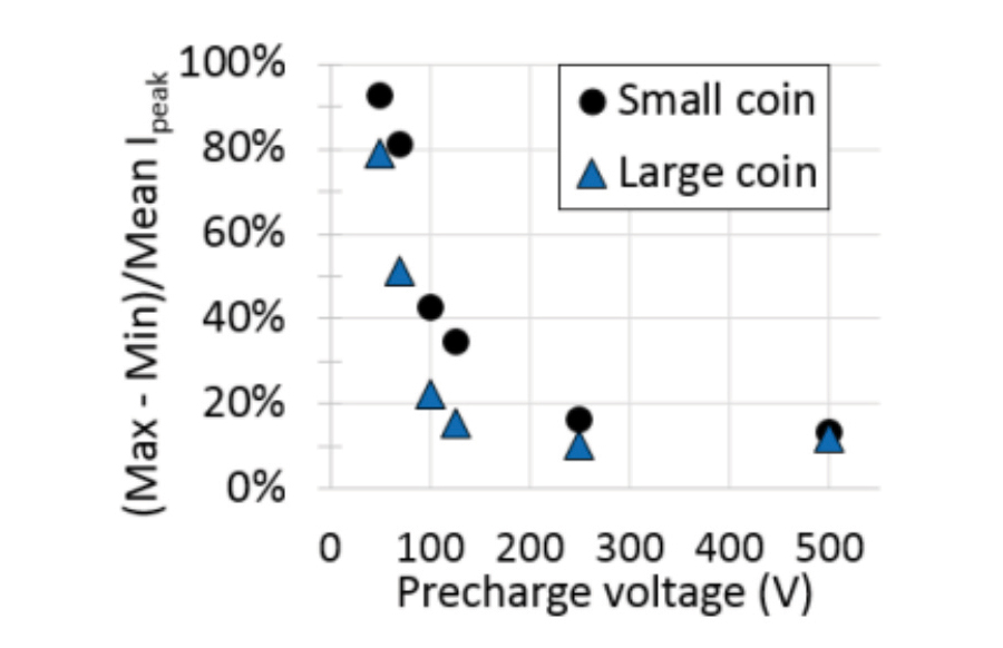
The reduced CDM passing levels of ICs below 250V (which are limited from the combination of large IC packages and high-frequency IC pins) must be measured accurately. ANSI/ESDA/JEDEC JS-002, published in 2015 by the EOS/ESD Association (ESDA) and updated in 2018 [7], is the most widely used field-induced CDM standard in the industry. It provides an extensive JEDEC CDM verification module waveform verification process combined with field-induced CDM tester hardware specification improvements, resulting in an improved accuracy test spanning over the CDM test range from 250 to 1000V. However, the inherent physical limitations of the air spark discharge, pogo pin alignment, and humidity result in increasing variation of peak current measurements at the lower charge voltages below 200V. In [8], Jack showed that the variation as a percentage of the mean increases significantly for pre-charge voltages below 200V (Figure 4).
chart showing the Ipeak maximum-minimum and the standard deviation of 50 zaps
Figure 4 (Jack, et al. [Jack 2015]): Ipeak maximum-minimum (top) and the standard deviation (bottom) of 50 zaps to JS-002 calibration coins as a percentage of the mean; 26% relative humidity. Data was taken on an Orion2 FICDM system using an 8 GHz oscilloscope.
In the field-induced CDM voltage range between 125 and 250V, this results in variations of more than +/- 50V, which greatly reduces the confidence of determining accurate CDM passing levels in the range between 125 and 250V. For example, single discharge testing between 200 and 250V often shows peak current waveform variability where one cannot tell the test voltage difference just from the waveform.

Fortunately, there are other CDM test methods in development that promise to deliver more reliable CDM test results. ANSI/ESDA/JEDEC SP5.3.3, Low Impedance Contact CDM [9] was published in 2018, which describes a contact-based method implementation of approximating the spark resistance of the field-induced method while eliminating the dependence on humidity. It has been shown to deliver repeatable, reproducible results in the 125V range and below (to 50V). Currently, the ESDA is conducting a worldwide multisite round-robin evaluation, a requirement leading to a path to a standard test method document -> inclusion as a full CDM test standard in the next 1-2 years.

Capacitively-coupled TLP (CC-TLP) [10] is another complementary method of contact mode stressing, delivering charging followed by similar CDM-like discharging, which has also been shown to be repeatable and reproducible with no dependence on humidity. A CC-TLP standard practice document is currently in review by the ESDA with a later 2021 release.

References
  1. T. Speakman, “A Model for Failure of Bipolar Silicon Integrated Circuits Subjected to Electrostatic Discharge,” Proc. of the IRPS, 1974.
  2. P. Bossard et al., “ESD Damage from Triboelectrically Charged Pins,” EOS/ESD Symposium, 1980.
  3. R. D. Enoch and R. N. Shaw, “An Experimental Validation of the Field-Induced ESD Model,” EOS/ESD Symposium, 1986.
  4. R. Renninger et al., “A Field-induced Charged-Device Model Simulator,” EOS/ESD Symposium, 1989.
  5. White Paper 2, “A Case for Lowering Component Level CDM ESD Specifications and Requirements,” http://www.esda.org/documents/IndustryCouncilWhitePaper2.pdf, alternately known as JEP157.
  6. White Paper 1, “A Case for Lowering Component Level HBM/MM ESD Specifications and Requirements,” http://www.esda.org/documents/WhitePaper1_HBM_MM_2010.pdf, alternately known as JEP155.
  7. EOS/ESD Association, ANSI/ESDA/JEDEC JS-002-2018, “Field-Induced Charged-Device Model Test for Electrostatic Discharge-Withstand Thresholds of Microelectronic Components,” 2018, available at http://www.esda.org.
  8. N. Jack and T. Maloney, “Low Impedance Contact CDM,” Electrical Overstress/Electrostatic Discharge Symposium Proceedings,” 2015.
  9. EOS/ESD Association, ANSI/ESDA/JEDEC SP5.3.3-2018, “Low-Impedance Contact CDM as an Alternative CDM Characterization Method,” 2018, available at http://www.esda.org.
  10. J. Weber et al, “Comparison of CDM and CC‑TLP Robustness for an Ultra-High-Speed Interface IC,” Electrical Overstress/Electrostatic Discharge Symposium Proceedings, 2018.

Share this story:
Charvaka Duvvury headshot
Charvaka Duvvury is a fellow of the IEEE and works as a technical consultant on ESD design methods and ESD qualification support. He has published over 150 papers in technical journals and conferences, holds numerous patents, and co-authored books on ESD design. He can be reached at cduvvury@gmail.com.
Alan Righter headshot
Alan Righter is a Senior Staff ESD Engineer in the Global ESD department at Analog Devices in Wilmington, MA. Alan Righter joined the EOS/ESD Association in 1997. Alan has been active in the EOS/ESD Symposium as author/co-author of multiple papers He can be reached at alan.righter@analog.com.
ESD Association logo
Founded in 1982, EOS/ESD Association, Inc. is a not for profit, professional organization, dedicated to education and furthering the technology Electrostatic Discharge (ESD) control and prevention. EOS/ESD Association, Inc. sponsors educational programs, develops ESD control and measurement standards, holds international technical symposiums, workshops, tutorials, and foster the exchange of technical information among its members and others.