he year was 2011, and an experiment was being done in China to record the effects of a triggered lightning flash on an overhead transmission line. The line was instrumented to record the induced currents, and the instruments were protected with a metal oxide varistor (MOV).1 The lightning flash recorded consisted of multiple return strokes, none of which exceeded the Imax rating of the MOV. But, much to the surprise of the experimenters, the MOV was damaged.
How could this happen? And more importantly, why might Imax not be a good basis for selecting an MOV for lightning protection, and are there alternatives? To help answer these questions, we’ll discuss in this article what an MOV is and how the way it is made influences its behavior when surged, how failures occur, and how multipulse surges differ from single surges in their effect on MOV properties.
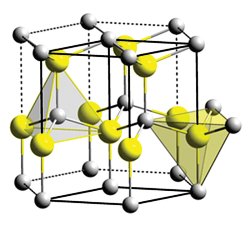
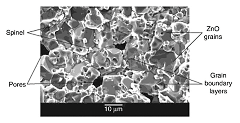
Second, a varistor is not one uniform wurtzite crystal, but many which coalesce into grains. To make ZnO into a varistor, a small amount of Bi2O3 is added. The Bi2O3 goes into the grain boundaries, as shown in Figure 2. In addition to Bi2O3, MnO may be added to enhance the nonlinear properties; Sb2O3 to control the ZnO grain growth; and a small amount of Al2O3 to increase the ZnO grain conductivity.
The Bi2O3 between two ZnO grains results in the formation of back-back Schottky diodes. So essentially, a varistor is a series-parallel arrangement of n-type material separated by back-back Schottky diodes having a voltage drop of about 2V-3V per grain boundary Junction (independent of grain size). According to He [1], this structure can be characterized electrically by Equation (1).

The first term in Equation (1) is seldom included in the V-I description of a varistor. It is the Schottky emission current in the low current region of the varistor. The second term is the usual nonlinear current in the high current region.
The constants in Equation (1) are controlled by varying the composition of the varistor material and sintering time of the manufacturing process. The threshold voltage Vth also depends on composition and sintering conditions. These control the number of grain boundaries between the two electrodes. Since Vth is proportional to the number of grain boundaries, more grain boundaries result in a higher Vth.
- The constants in a varistor model like Equation (1) are likely to be different for every varistor; and
- Not all varistors of the same dimensions have the same properties – an important consideration when choosing a MOV for protection.
The energy absorption capability can be divided into thermal energy absorption capability and impulse energy absorption capability. Impulse energy absorption capability depends on how the impulse is applied:
- Single impulse stress
- Multiple impulse stress (without sufficient cooling between the impulses)
- Repeated impulse stress (with sufficient cooling between the stresses)
Thermal energy absorption capability, on the other hand, is mainly affected by the heat dissipation capability of the overall arrester design, in addition to the electrical properties of the varistors.
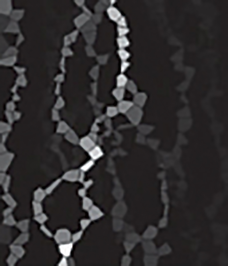
Let’s first consider varistor failure caused by heating. At lower currents, the heating localizes in strings of tiny hot spots, which occur at the grain boundaries where the potential is dropped across Schottky-type barriers (see Figure 3). The heat transfer, in this case, is too fast to permit temperature differences that could cause failure.
Now consider higher currents. In small varistors (e.g., <25 mm) where the number of ZnO grains between the electrodes might be only about 40, a variation of 3 – 4 grains can cause the current flow in a given path to be an order of magnitude different from surrounding paths. The paths with low breakdown voltages carry most of the current and become hotter, with consequences noted in the study of Sargent et al [4]. In that study, analysis of the failed MOV samples showed cracking and a formation of new amorphous material near the conduction channel. Examination of this amorphous material suggested that local hot spots (actually hot channels) were formed when the energy resulting from a current pulse applied to the MOV was absorbed faster than it could be dissipated. The amorphous material in these hot spots likely resulted from a plasma formed during the current pulse. The hot spots rapidly cooled afterward due to heat conduction to the surrounding ZnO grains.
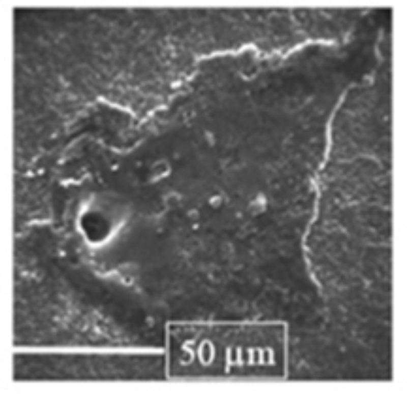
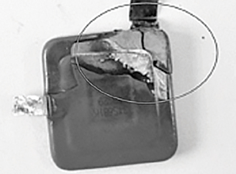
Under different current conditions, failure modes include electrical puncture (see Figure 4), physical cracking (see Figure 5), and thermal runaway. Cracking happens because varistors are basically a ceramic material, and hitting them with a sharp high-amplitude surge is like hitting a dinner plate with a hammer.
If the current is continued long enough, the energy deposited in the varistor may raise its temperature to the point of thermal runaway due to the material’s negative temperature coefficient of resistivity [1].
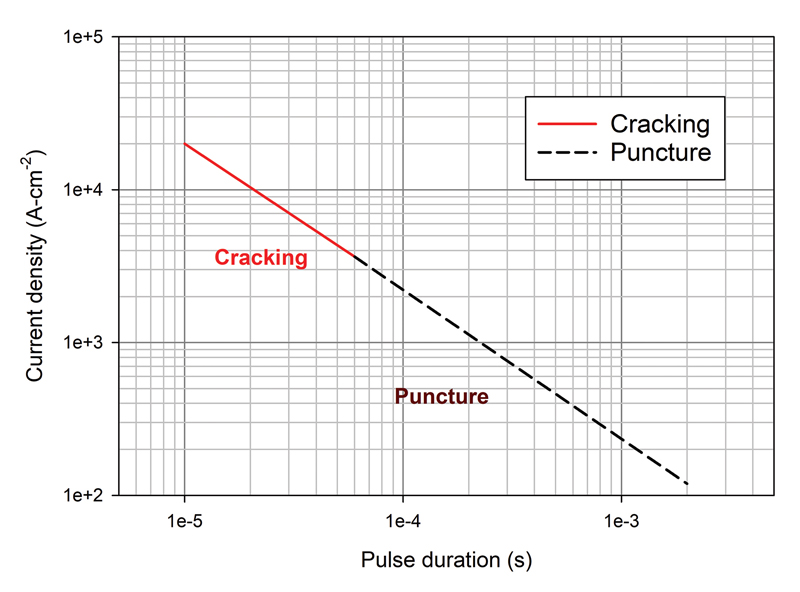
Figure 6 illustrates the conditions under which cracking and puncture can occur. For a given varistor, the red solid line shows cases under which cracking might occur, and the black dashed line cases under which puncture might occur.
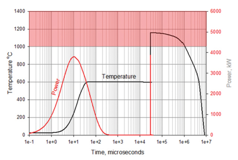
As noted previously, in the study of Sargent et al, analysis of the failed 18 mm MOV samples subjected to a multipulse burst test showed the formation near the conduction channel of a new amorphous material, which was thought to require a local temperature around 1000° C. Thermal modeling suggested that this temperature rise would occur if the pulse power was concentrated in about 2% of the MOV volume. This is an important observation because a calculation of the energy absorbed in the multipulse burst test showed that the temperature rise of the MOV would only have been 231° C if the temperature distribution were uniform, much less than the temperature thought to have caused the damage.
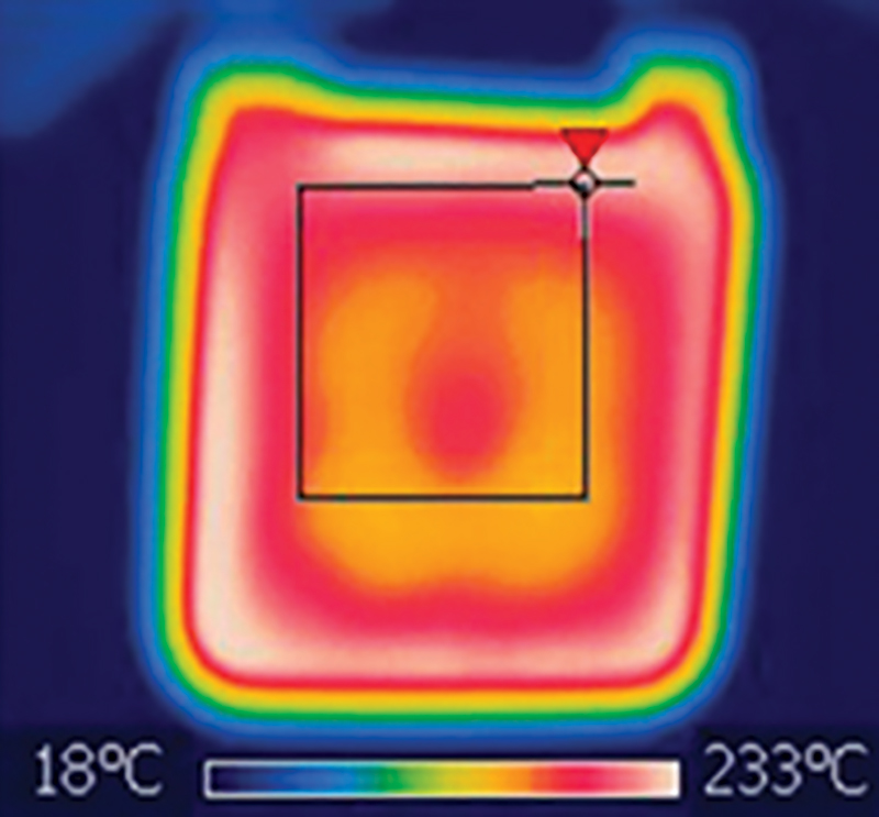
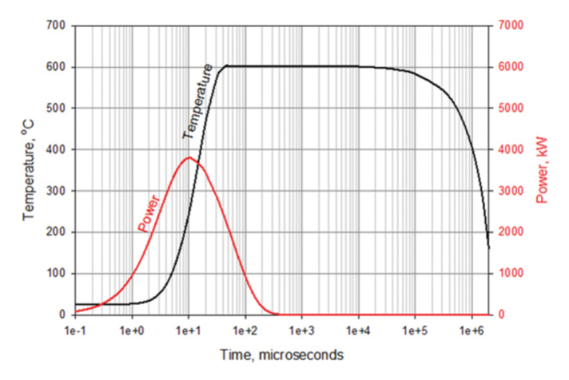
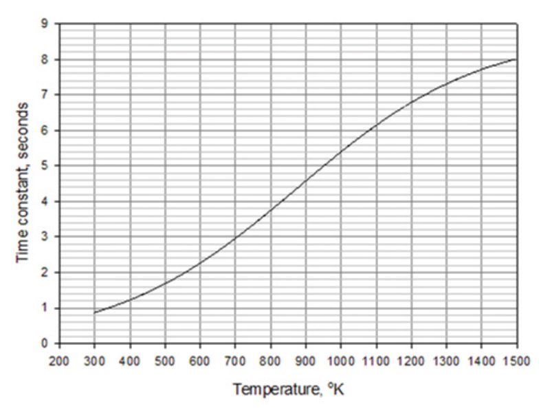
The results of Sargent et al suggest that the criterion for failure of an MOV is a localized temperature rise to 1000° C (or the vicinity thereof). So for an MOV under consideration, we need to determine if a localized area might reach 1000° C. Figure 11 shows the additional temperature rise that happens when the surge used to create Figure 10 is applied to the same MOV a second time after 30 ms. The additional temperature rise is due to the relatively long thermal time constant of the MOV, which prevents the MOV from dissipating much heat energy (and hence cooling) before the second surge arrives. The temperature rise is now in the red area above 1000° C, where failure is expected. So this is an example of how a varistor can be destroyed by multipulse surges.
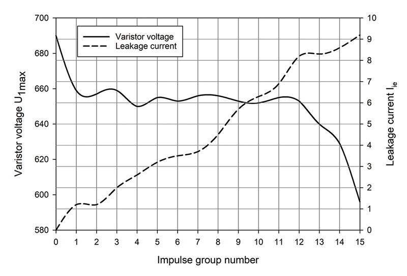
In another look at the effects of multipulse lightning, a study by Zhang et al [5] explored the progression of failure in varistors under multiple lightning strokes, using a series of five-pulse groups of 8/20 lightning surges having pulse intervals of 50 ms and pulse amplitudes set at the 20 kA nominal discharge current. The time between the application of one group of impulse currents to a varistor and that of the next group of impulse currents was 30 minutes, allowing a return to the original conditions.
So it is possible that a single non-destructive multipulse burst conditions the MOV for failure from future multipulse bursts, as suggested by the continually increasing leakage current. This conditioning could be viewed as a kind of accelerated wear-out process.
Microstructural examination of the failed varistors indicated that after the multiple lightning strokes, the grain size decreased and the proportion of Bi in the grain boundary layer increased significantly. These effects were the cumulative result of multiple lightning currents, and were caused by thermal damage and grain boundary structure damage due to temperature gradient thermal stress. This damage eventually led to failure of the MOV. Note that a single surge test would miss this wear-out mechanism.
High amplitude short-duration single pulse tests (e.g., 6 kV, 3kA 8/20) are typically used to evaluate varistor failure. This type of test may cause a failure mode different from that in a varistor subjected to multipulse lightning at lower amplitude (e.g., cracking vs. wear-out). Single-pulse tests could also miss heat accumulation failures that multipulse lightning can cause, especially multipulse lightning that includes continuing current.
As pointed out in [10], what caused failure was the continuing current part of the multipulse sequence, and continuing current is not comprehended in the Imax rating. The continuing current deposited enough energy in the MOV to fail it.
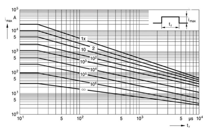
Similarly, the amplitude of the current would be decreased such that a for the two-hit line, a second group of surges would cause failure on the third application, and the process repeated using groups of surges with wider waveshapes. This process would be continued until enough lines had been generated to adequately characterize the product.
In the case of short-duration high amplitude surges, MOV failure may occur by cracking before melting happens. Single short-duration high amplitude surges might occur on power lines, so MOV ratings established this way can be appropriate for power-line applications
For protection against lightning, ratings established by multipulse testing may be more important. This is because a multipulse lightning surge is often the driver for the temperature rise since it causes energy to accumulate in the MOV due to its long thermal time constant. This is why multipulse testing is important since a single surge test might miss failures that multipulse lightning can cause, notably wear-out, and especially multipulse lightning that includes continuing current. And most lightning is of the multipulse type. The microstructure degradation effect of repeated multipulse surges may need to be considered when constructing derating curves.
Understanding the mechanism of how surging an MOV alters its microstructure is important to understanding how MOVs fail. It is a topic that needs further research.
- Jinliang He, Metal Oxide Varistors: From Microstructure to Macro-Characteristics, John Wiley and Sons, 2019
- M. Bartkowiak, “Current Localization, Non-Uniform Heating, and Failures oF ZnO Varistors,” Fall Meeting of the Materials Research Society, Boston, MA, December 1-5, 1997
- Gordon Pike, “Breakdown in ZnO Varistors by High Power Electrical Pulses,” Sandia Report SAND2001-2160, July 2001.
- R. A. Sargent, G. L. Dunlop and M. Darveniza. “Effects of Multiple Impulse Currents on the Microstructure and Electrical Properties of Metal-oxide Varistors”, IEEE Transactions on Electrical Insulation Vol. 27 No. 3, June 1992.
- Chunlong Zhang, Hongyan Xing, Pengfei Li, Chunying Li, Dongbo Lv and Shaojie Yang, “An Experimental Study of the Failure Mode of ZnO Varistors Under Multiple Lightning Strokes,” Electronics, February 2019.
- CIGRE WG C4.407, “TB549 Lightning Parameters for Engineering Applications,” 2013.
- A. Rousseau, X. Zhang, and M. Tao, “Multiple Shots on SPDs – Additional Tests,” International Conference on Lightning Protection (ICLP), Shanghai, 2014.
- A.R. Martin, “Effects of Multi-burst Lightning Flashes on Surge Protective Devices using MOVs,” In Compliance Magazine, November 2017, pp32-39.
- S. J. Yang, S. D. Chen, Y. J. Zhang, W.S. Dong, J. G. Wang, M. Zhou, D. Zheng, and H. Y Hui, “Triggered Lightning Analysis Gives New Insight into Over Current Effects on Surge Protective Devices,” http://www.ten350.com/papers/icae-conghua.pdf, 2011.
- M. Maytum, “CIGRÉ (Council on Large Electric Systems) Technical Bulletin (TB) 549 (2013) Lightning Parameters for Engineering Applications,” The Alliance for Telecommunications Industry Solutions Protection Engineers Group Conference, Littleton, CO, 2014.
- IEEE PC62.33 ™ Standard for Test Methods and Performance Values for Metal-Oxide Varistor Surge Protective Components
- A varistor is often called an MOV (Metal Oxide Varistor)
- E is the excitation energy of varistor, K Boltzmann’s constant, A1, A2, and m are constants related to the electrical characteristics of varistor, Vth is the threshold voltage.

