Application of Thrifty Test Equipment for EMC Testing
Low-Cost Instruments and Procedures to Troubleshoot EMC Issues
money sign with electrical battery lines attached
I

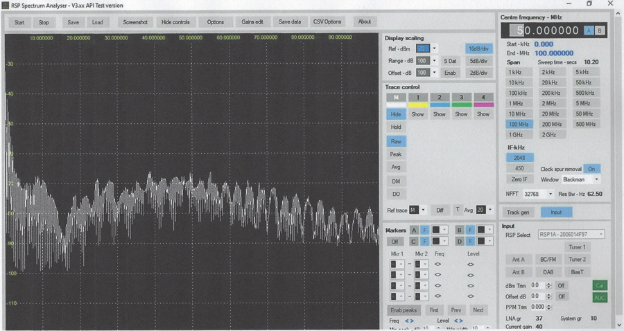
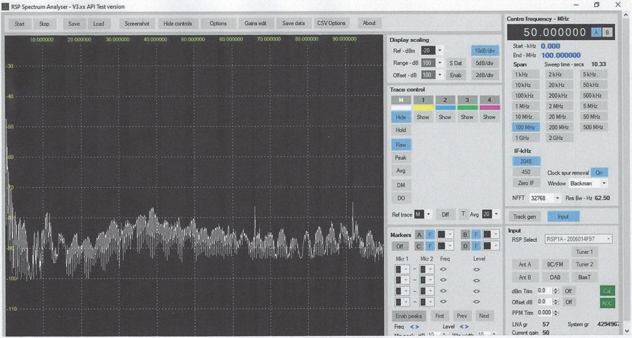
ssues related to electromagnetic compatibility (EMC) are often identified during qualification testing in an accredited EMC test lab which typically occurs late in the product design cycle. Obtaining a cost-effective solution to these EMC issues may be time-consuming, and many EMC labs can be fully booked or have limited availability, have long lead times, or involve significant costs. But inexpensive test equipment and procedures (let’s call them thrifty methods) used for helping to solve these EMC issues outside an EMC lab are very desirable, especially if no in-house EMC facilities are readily available.

There are several excellent resources for troubleshooting methods and building a low-cost EMC toolkit.1 This article offers some other test equipment options that have different capabilities and which can be even less costly. Although the thrifty method is mainly used to compare results before and after implementing a fix (not meeting a specification limit), with some experience, it can also be used in the pre-qualification development stage early in the design cycle to identify potential issues before formal lab testing. Identifying issues early allows maximum flexibility to experiment and provides sufficient time to make cost‑effective changes before a design is frozen and difficult to change.

Thrifty Test Equipment
Vector Network Analyzer
One of the low-cost instruments discussed in this article is a vector network analyzer (VNA). Figure 1 shows an example of such an instrument (the NanoVNA2). Even though this VNA typically costs less than $150, it is useful from 50 kHz to 3 GHz and comes with cables and calibration terminations. It can be used as a standalone unit via touchscreen, but it is best used with free software QT and Saver. Although this VNA has a lot of capability, I used it for input impedance (S11) and VSWR measurements in the testing on which this article is based.
Vector network analyzer
Figure 1: Vector network analyzer
Software Defined Radio
Figure 2 shows another low-cost instrument, a software defined radio (the SDRplay3). Also, typically less than $150, most SDRs also offer lots of capabilities. For the purposes of this article, we’ll use the SDR as a spectrum analyzer with the addition of another free software program (Spectrum Analyzer 1.1). While this software may have limitations, such as only fixed frequency spans, it can still be very effective.
Software defined radio
Figure 2: Software defined radio
RF Signal Amplifier
A radio frequency (RF) signal amplifier is required for radiated emissions measurements. Figure 3 shows one low-cost example. This particular unit uses a monolithic microwave integrated circuit (MMIC) amplifier and is useful from 50 kHz to at least 2 GHz, Gain = 20-30 dB, and only costs about $30. For a device under test (DUT) with very low emission limits, two amplifiers in series may be required.
RF signal amplifier
Figure 3: RF signal amplifier
RF Power Amplifier
For radiated immunity (e.g., in this article, bulk current injection, or BCI), an RF power amplifier is required. Figure 4 shows one example (NWDZ-RF-PA) that covers 2 – 700 MHz and is about $25. This particular unit uses a SBA5089Z amplifier IC and RD01MUS1 MOS FET. However, the MOS FET overheats which, can be corrected by changing the bias on its gate (R6 changed from 5k ohms to 3.3k ohms).
RF power amplifier
Figure 4: RF power amplifier
RF Signal Generator
Another tool in our thrifty set is an RF signal generator. The example shown in Figure 5 (TinySA4) has an amazing set of capabilities and only costs about $85. Although its main function is that of a spectrum analyzer, we’ll use it in testing described in this article as an RF signal generator. The unit has two outputs. The high output is a square wave, which covers 240 – 960 MHz, and the low output is a sinewave and covers 0.1 – 350 MHz. This low output is the one to be used here and is easily configurable by the touchscreen for amplitude (up to -7 dBm, 1 or 10dB steps), frequency, CW, sweep, and modulation.
RF signal generator
Figure 5: RF signal generator
TEM Cell Variant
Radiated emissions are often the most common issue. In general, near-field probing correlation with EMC lab testing can be poor. Even if near-field probing indicates the potential source of the emissions and a fix is implemented, lab chamber radiated emissions testing may not show any improvement. This is due to the many coupling mechanisms involved from the noise source to the PCB, housing, and wiring harness.
DIY TEM cell variant (front door removed)
Figure 6a: DIY TEM cell variant (front door removed)
To evaluate radiated emissions, I’ve used a variation of a TEM cell (see Figure 6a-c) for over a decade. Such an enclosure is required to keep out ambient radiation such as AM/FM radio. Although you cannot compare results on an absolute level as those obtainable in an EMC lab anechoic chamber, the use of a TEM cell shows similar trends. For example, if the improvement for a particular fix is x dB, there will be similar improvement in an EMC lab chamber.
DIY TEM cell variant (sliding door in place)
Figure 6b: DIY TEM cell variant (sliding door in place)
This homemade cell is made from HVAC sheet metal ducting available at many home improvement stores. The dimensions are 16 x 16 x 37 inches, with a center plate (without end tapers) of 32 x 13.5 inches. The center plate height is adjustable to accommodate different DUT sizes (default is in center between top and bottom). Figure 6b shows a small opening in the door. This opening is to help isolate the source of the noise (DUT, harness, or both) by allowing placement of the harness outside the TEM cell.
TEM cell variant, end taper and BNC connection detail
Figure 6c: TEM cell variant, end taper and BNC connection detail
In Figure 6d, looking at the S11 and voltage standing wave ratio (VSWR), it appears that this TEM cell is only useful for frequencies less than about 200 MHz. However, it has been used with success in finding fixes for frequencies greater than 1 GHz. Since we are only using the TEM cell to assess before and after results from any fixes, any discrepancies can usually be ignored as long as the DUT and harness locations are controlled (i.e., consistency in DUT positioning and orientation). In an anechoic chamber, the antenna is much farther from the DUT and harness than in this homemade chamber, and proximity coupling with DUT variation is less of an issue.
VNA results for TEM cell (Saver software)
Figure 6d: VNA results for TEM cell (Saver software)
Bulk Current Injection (BCI) Probe
If issues have been identified in EMC lab testing for bulk current injection (BCI), a thrifty method of investigating and possibly solving these issues can be of great value. A low-cost version can be made from a ferrite current clamp as shown in Figure 7a.5 Using the VNA mentioned previously in this article, I was able to determine that anything over one turn was detrimental. Figure 7b for one turn shows a reasonable impedance and VSWR, but Figure 7c illustrates how these values get much worse even after just two turns.
DIY bulk current injection probe (single turn) for radiated immunity
Figure 7a: DIY bulk current injection probe (single turn) for radiated immunity
BCI injection probe (single turn, Figure 7a) VNA measurements
Figure 7b: BCI injection probe (single turn, Figure 7a) VNA measurements
BCI injection probe (two widely spaced turns) VNA measurements
Figure 7c: BCI injection probe (two widely spaced turns) VNA measurements
Figure 7d shows a calibration setup using a signal generator feeding an RF power amp whose output feeds a 3 dB attenuator and the BCI probe. The induced current is measured with a cheap version of the BCI calibration jig. The voltage is measured across a 50-ohm, 10 dB attenuator leading to the spectrum analyzer. Induced current was measured at over 2 – 350 MHz, and the maximum is about 100 mA rms which is similar to what is required to meet most automotive EMC specifications.
BCI calibration setup
Figure 7d: BCI calibration setup
ESD Simulator
A piezoelectric barbecue lighter like that shown in Figure 8a has been suggested as a low-cost ESD simulator. However, based on verification testing I conducted in a commercial EMC test lab, this lighter has much lower energy than a commercial ESD gun like that shown in Figure 8b, I compared both the piezoelectric simulator and an ESD gun with a calibration target (e.g., IEC 61000-4-2) and high frequency scope. The piezoelectric simulator has no control for magnitude and repeatability. The ESD example in the next section of this article shows that it is important to quantify ESD parameters. Unfortunately, there is no low-cost version of a commercial ESD gun in this case.
ESD low-cost simulator
Figure 8a: ESD low-cost simulator
ESD gun example
Figure 8b: ESD gun example
Product Application Examples
Figures 9a-c and Figures 10a‑b on pages 94 and 95 illustrate thrifty TEM cell results before and after fixes were applied to two different automotive devices. These examples illustrate that the TEM cell setup is valid for a wide frequency range. Before the fixes, neither meet the auto manufacturers’ EMC specification limits. But after, they both did as verified in an EMC lab. Figure 9a shows a typical setup with the DUT, wiring harness and battery within the TEM cell.
Example 1—Module A, TEM cell setup
Figure 9a: Example 1—Module A, TEM cell setup
Example 1—Module A, without fixes, 0 - 100 MHz (20 dB external amp)
Figure 9b: Example 1—Module A, without fixes, 0 – 100 MHz (20 dB external amp)
Example 1—Module A, with EMC fixes
Figure 9c: Example 1—Module A, with EMC fixes
Example 2—Module B, without fixes, 1530 - 1630 MHz (2 x 20 dB external amps)
Figure 10a: Example 2—Module B, without fixes, 1530 – 1630 MHz (2 x 20 dB external amps)
Example 2—Module B, with EMC fixes
Figure 10b: Example 2—Module B, with EMC fixes
Automotive LED Taillight, ESD
This example is based on an actual case in the field. It was originally thought that power line voltage transients were the cause of the issue. We conducted testing using transients specified in SAE J2628.6,7 These transients are very realistic and severe but could not precipitate the issue.

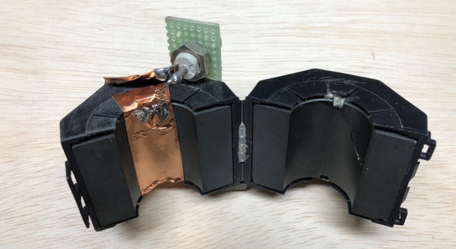
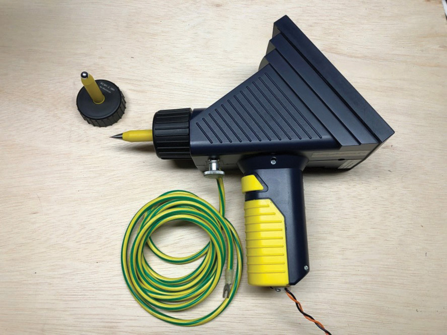
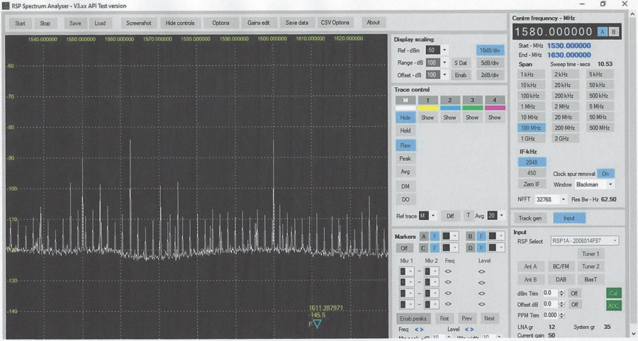
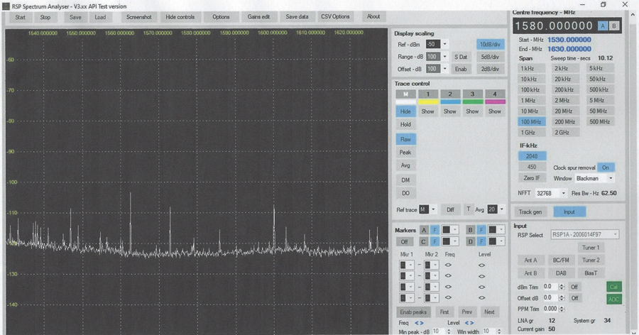
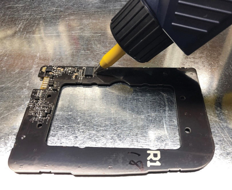
The next potential culprit was thought to be due to ESD. Testing as shown in Figure 11 (PCB over ground plane) showed that this was indeed the root cause problem. The ESD gun was applied directly to each pin of the suspect IC (air discharge not repeatable). The IC had one pin that had much lower immunity (< 2 kV, one discharge) than the other pins (> 6 kV, multiple discharges). To determine this immunity, many PCBs were sacrificed.

ESD gun applied to IC pins
Figure 11: ESD gun applied to IC pins
Summary and Conclusion
In this article, we’ve presented a number of effective low-cost (thrifty) test instruments that can be used for EMC testing for both pre-qualification and troubleshooting, along with application examples that validate their usefulness. These options can enable you to resolve design potential issues efficiently without the time and cost constraints of an EMC test laboratory.
Endnotes
  1. See, for example, EMI Troubleshooting Cookbook for Product Designers by Patrick G. Andre and Kenneth Wyatt.
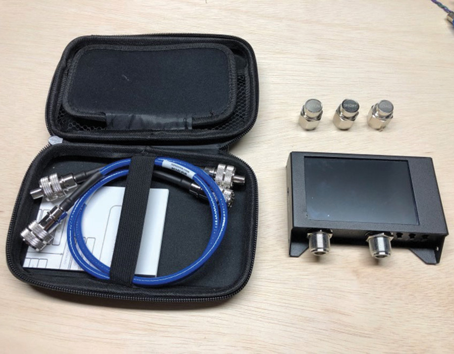
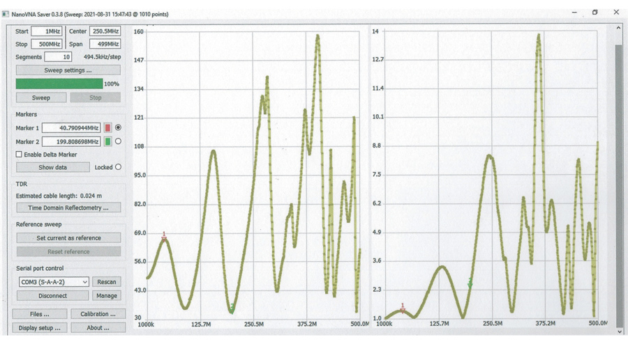
  2. Detailed information about the NanoVNA is available at https://nanorfe.com.
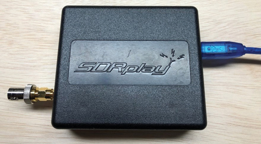
  3. Detailed information about the SDRplay is available at https://www.sdrplay.com.
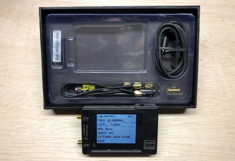
  4. Detailed information about the TinySA is available at https://www.tinysa.org/wiki.
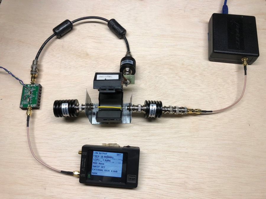
  5. See “Injection Probe Modeling for Bulk Current Injection Test on Multi Conductor Transmission Lines” by Frédéric Lafon, Younes Benlakhouy, and François de Daran for a cut-away of the BCI probe shown in Figure 7a.
  6. SAE J2628, Characterization, Conducted Immunity.
  7. For a detailed comparison of these transients and ISO 7637‑2, see “Comparison of ISO 7637 Transient Waveforms to Real World Automotive Transient Phenomena” by Keith Frazier and Sheran Alles, 2005 IEEE EMC Symposium.
Share this story:
Arnold Nielsen headshot
Arnold Nielsen is an iNARTE-certified EMC design engineer with decades of experience in the automotive electronics industry. He currently consults on a wide variety of products and can be reached at arnienielsen@gmail.com.