ver the last decade, automotive original equipment manufacturers (OEMs) like Ford, GM, and Tesla have been at the forefront of mobility and advanced driver assistance systems (ADAS), jockeying for a leadership position in this hotly contested, quickly developing field. As these systems advance, with them comes an increase in the number of semiconductor components in the vehicle to support devices like cameras, radars, and modules used to make decisions based on their information.
This has provided an opportunity for semiconductor manufacturers to increase their market share, allowing them to pivot from their traditional base microcontroller (MCU) offerings to highly integrated system on chip (SoC) processors, memory, and power devices. However, as the industry evolves, the question remains for both consumers and OEMs alike, “How can we standardize the development and design of these components across the industry, such that we can satisfy the risk that comes along with these components, while confidently claiming the part functionally safe?”
Enter the first edition of ISO 26262, Road vehicles—Functional Safety, which was the industry’s attempt at standardizing the development of the components of these large systems to minimize both:
- Systematic risk, errors generated in the design process through a missed requirement cascade or an incomplete analysis; and
- Random hardware faults specific to the malfunction of the device in question.
For roughly the last decade, automotive OEMs have been relying on part 5 of this standard to help them address hardware malfunction at the component level and to establish what the industry considers safe design practices. The result of this analysis has led the industry to focus mostly on the core of each electronic module, the microcontroller, in addition to adopting the failure mode effects and diagnostic analysis report, dependent failure analysis, and their peer reviews.
And this is how engine, gateway, and body controllers coalesced around what is considered mostly common for functionally safe electronic control units (ECUs). They employ things like dual core lockstep processors, double stored variables, and other safety mechanisms that enhance their coverage metrics to achieve the all-important Automotive Safety Integration Level (ASIL) rating. Building upon part 5 of the standard, and the level of complexity to which automotive systems have ascended, ISO 26262 has expanded its coverage to include part 11, which focuses on semiconductor components, with the goal of simplifying the automotive system by both:
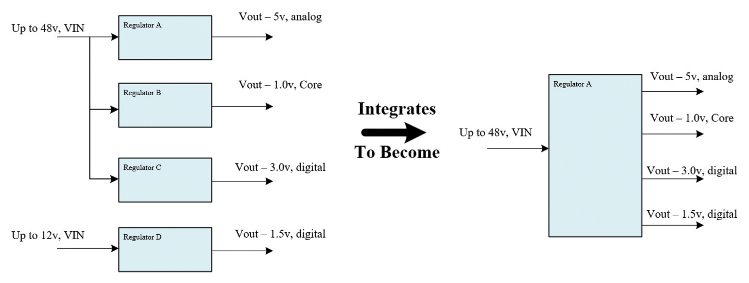
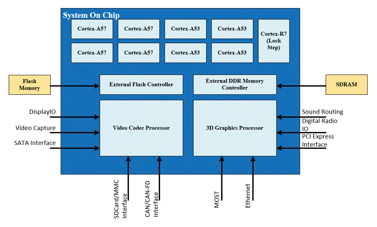
- Combining multiple functions into one large system on chip, thereby creating large SoC devices with multiple power domains, and
- Wanting to simplify wiring such that only one low voltage bus runs throughout the vehicle.
An example of this integration is shown in Figure 1.
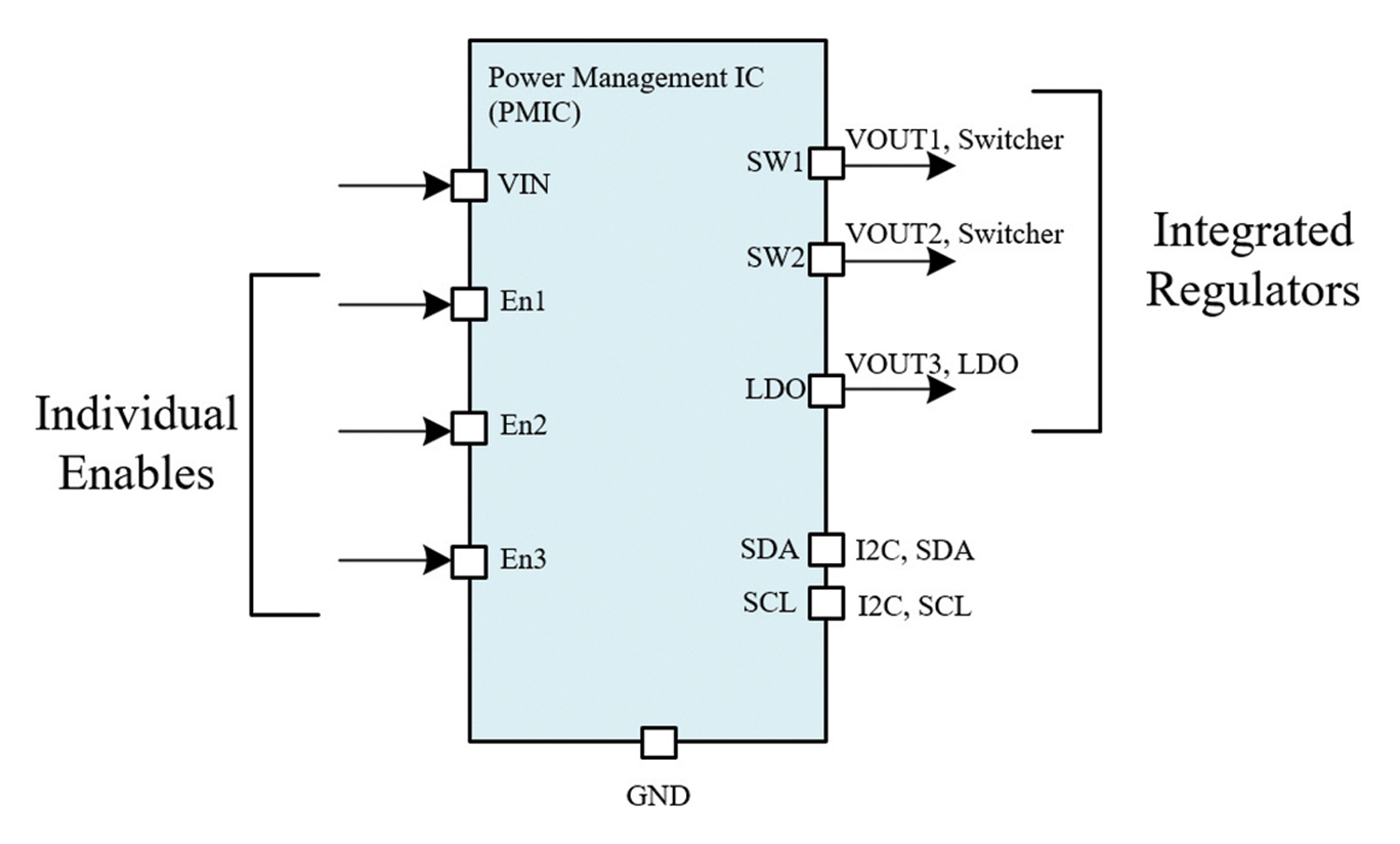
This leads automotive system designers to adopt multi-rail, high power, power management devices (PMICs) that have traditionally been reserved for high-end server systems and other highly integrated consumer devices. These devices are capable of splitting one voltage rail into multiple lower voltage rails via integrated switching and linear regulators, in addition to being able to monitor each output. But semiconductor manufacturers who’ve normally prioritized speed in development to get into a next-generation server socket and are now tasked with applying part 11 to their products, with customers left to determine how to implement them.
To help automotive designers understand what to look for when shopping for PMICs and other power devices, we’ll use an analysis containing a hypothetical situation that starts with a simple quality managed (QM) switching architecture for a basic DC/DC converter, then apply the tools ISO 26262 gives us to analyze the possible failures and, finally, present an architecture that attempts to address dependent and random hardware failures. It’s important to note that many solutions to the “What makes this device safe?” question exist, so the analysis and mechanisms discussed here are common.
This article isn’t meant to be conclusive, and a lot depends on what extra functions are required of the device by the system integrator. But this article will allow you, the automotive module designer or safety manager, to recognize what to look for when shopping for your next power device for your module.
In reading through ISO 26262, the standard suggests three widely accepted analysis tools that help the safety manager lead the design team to an understanding of how to create a functionally safe product. These tools are:
- The block diagram;
- The failure mode effects and diagnostic analysis (FMEDA); and
- The dependent failure analysis (DFA).
These tools are suggested for their ability to reduce complexity and allow the team performing the analysis to confidently arrive at a functionally safe design. In this article, we’ll review each technique, give examples of how they’re used, and then apply them in the safety analysis.
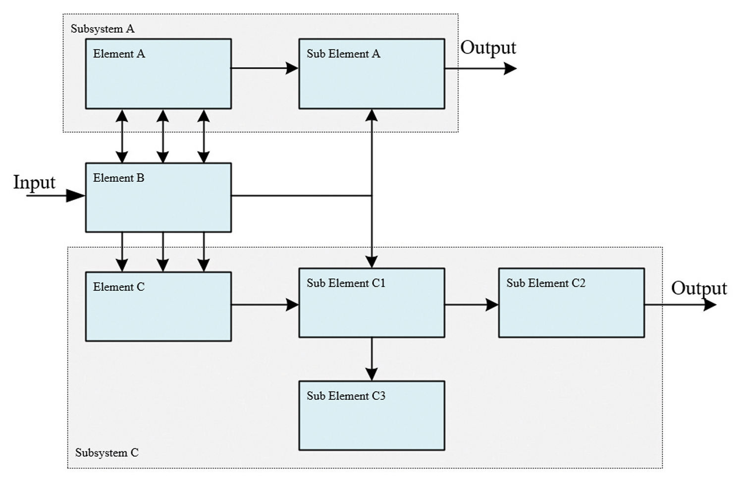
- Abstract the design to ensure that each block has a dedicated function, eliminating the need for needless (and often confusing) mixing of functions, and forcing the designer to plan their design prior to implementing it; and
- Allow the conceptual safety analysis to easily understand information flow and determine where mechanisms need to be implemented, and the design decisions that need to be made in order to create a design free from dependency.
A simple example of such a diagram is shown in Figure 4.
When establishing a hierarchy, it’s important to remember. Abstraction! Without it, the diagram loses context and becomes a burden to maintain and develop. A recommended rule of thumb is to create a hierarchy not more than three to four sublevels deep, with the goal being to be able to have enough detail such that the box being described becomes self‑describing.
- The dependent failure analysis: This analysis tool is designed to help identify dependent failures between safety mechanisms and components they’re meant to protect, this is largely requirements driven and is dependent upon the system safety goals.
- The failure mode effects and diagnostic analysis: This analysis tool takes into account commonly accepted failure modes such as broken resistor strings and component drift and determines the impact on function of the device. It is also used as a calculator, justifying your safety coverage for an ASIL rating.
These dependencies and failure modes are analyzed within the context of the stated safety goal of the device. The safety goal is the primary high-level safety related function that the device is designed to support. In most power management devices, at the PMIC component level this goal relates to output power monitoring which plays an important role in supporting the system safety concept; this is usually defined in context higher-level function such as providing a self-driving function.
In this article, our example safety goal is to monitor the output for any voltage irregularities and provide a means to notify the system when we’re unable to provide this support properly such that they can suspend any safety-related decisions that might be impacted by an output failure.
For the safety manager evaluating devices for potential use in their module, they’re mostly concerned with voltage drift, spikes, and oscillations of the output rail, while maintaining the ability to warn the system if any of these occur.
- VCC and ground circuits: Where drifts, noise, or failures of circuits powering the safety mechanism and the device it powers could adversely impact both.
- Temperature: Where an increase or decrease in temperature could impact a mechanism’s monitoring accuracy while at the same time decreasing its ability to control something.
- Shared components: Where the failure of components like memory buses and other shared devices could impact both a monitor and regulator function.
The DFA helps a design to become free from interference by obtaining dependence, as shown in Figure 5, by addressing cascading faults and common cause faults (CCF).
Companies that have implemented a culture of safety in their design process have defined initiators that that are meant to help guide the design and safety teams in their analysis.
- Resistor failures and component drift
- Soft error rate in memory, and stuck at faults in digital logic circuits
- Data transmission failures, including loss of message, corrupted messages, and unintended message
In the conceptual phase, these faults are applied to the design, mechanisms are created to address the failure modes, and then a quantitative analysis is conducted to determine exactly how well the mechanism addresses the failure mode. The DFA is conducted to ensure that the device addresses dependencies.
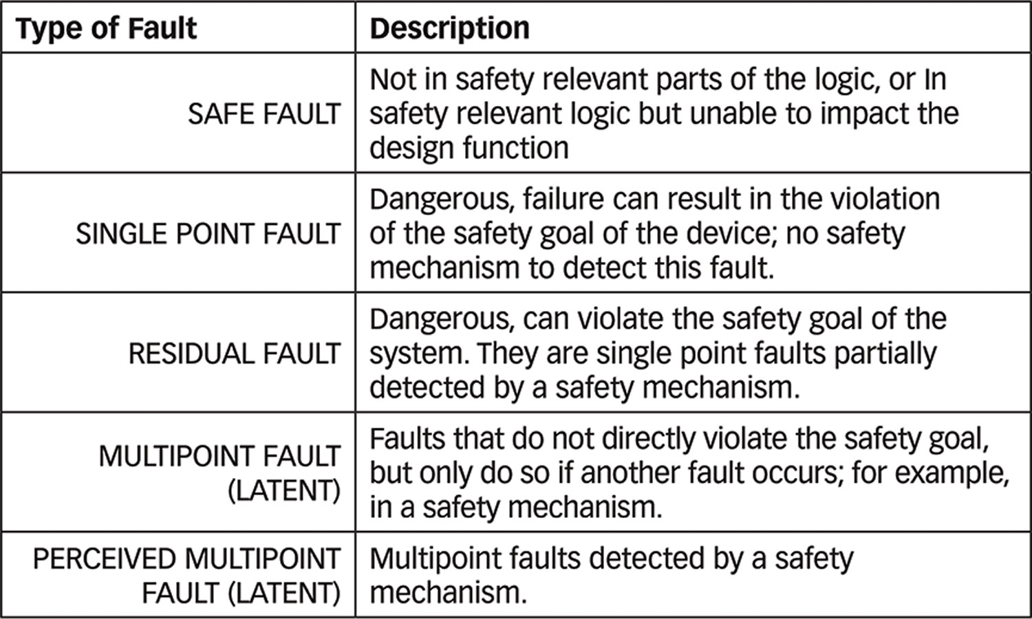
The FMEDA considers faults into multiple classes, two of which include:
- Single point failure mode (SPFM), where the failure of the circuit or device directly impacts the ability for the device to perform a task related to the stated safety goals. An example would be a feedback control loop opening leading to oscillatory behavior.
- Latent fault (LF) failure mode, where the failure of the circuit or device indirectly impacts the ability for the device to perform a task related to the stated safety goal. An example would be a monitor that only outputs no fault due to a short circuit failure; it requires a fault to be impactful to the system.
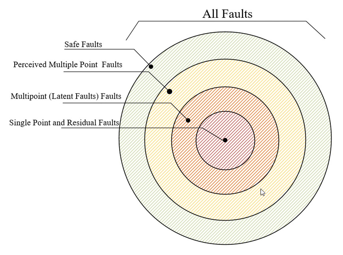
Table 1/Figure 6: Types of faults
Latent faults are more nuanced, as their occurrence alone is not enough to impact the function of the system as it relates to the safety goal and requires as a single point fault for impact. Conversely, a single point fault’s impact will directly impact the it [the safety goal]. A more complete fault classification is contained Table 1/Figure 6.
The challenges of a FEMDA stem from the fact that it’s meant to be an exhaustive analysis. In devices that implement a large number of discrete components (e.g., millions of transistors) it can be a daunting task, which is why it’s often paired with a DFA for an exhaustive analysis. The effectiveness of the DFA and FEMDA all depend on how well the design is understood at the time of analysis, which is even more reason for a disciplined design group to have a well thought out design.
Next, we’ll use these three tools in analyzing, and creating a functionally safe power management device.
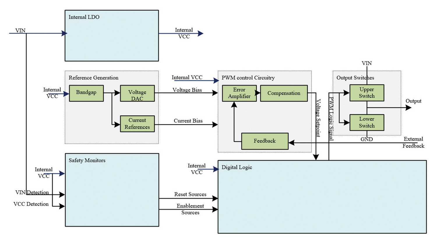
Introducing the Basic DC/DC Converter Architecture
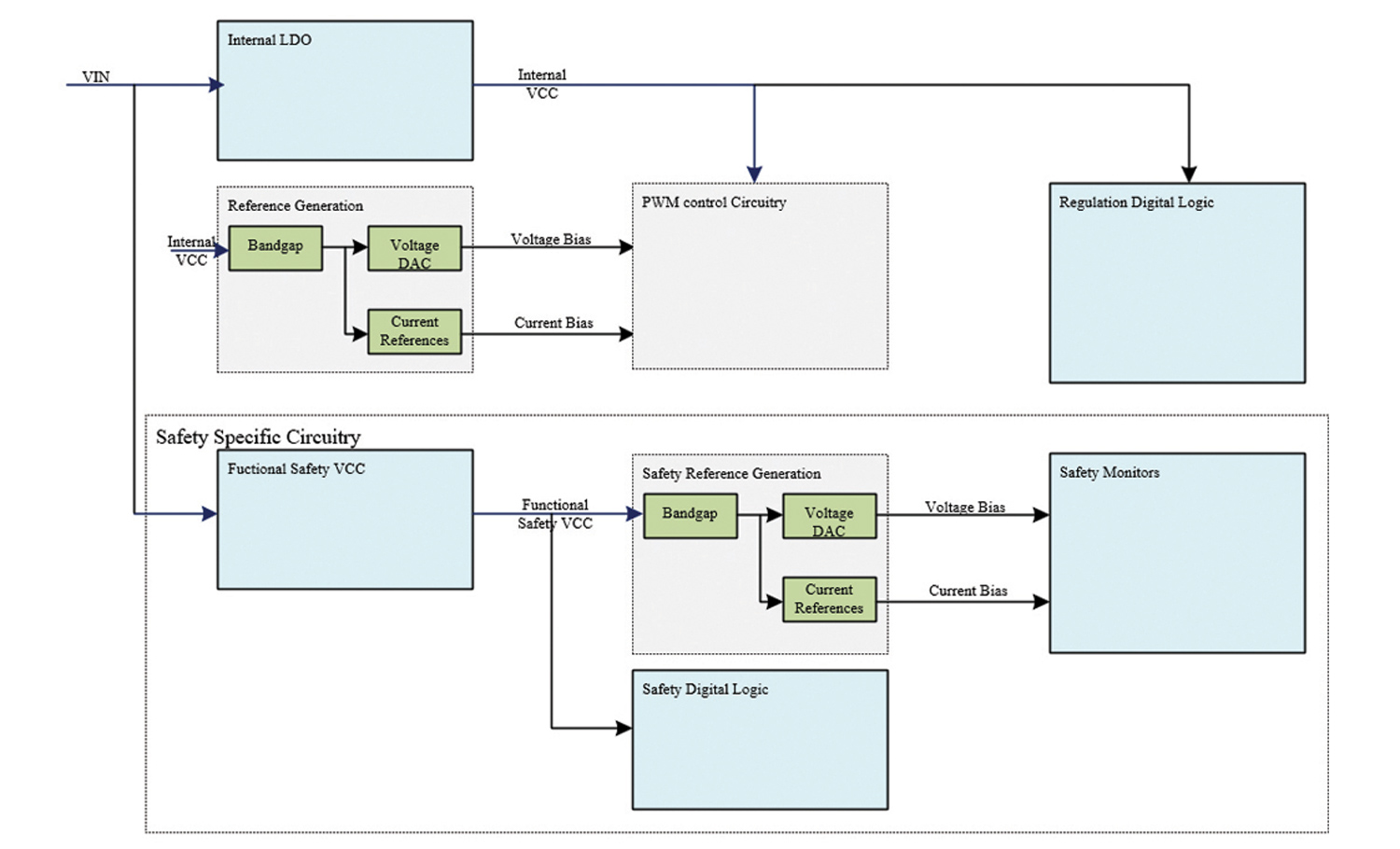
- Voltage reference generation: This normally includes the bandgap, and a digital to analog converter that provides references to switching converter, monitors, and any other devices that need a bias current or voltage.
- Internal rail generation: The internal power domain that provides power to the internal components of the device and sets the voltage input/output (VIO) level.
- The switches: These devices span the range of implementation, but in general, this includes the pre-driver and driver circuitry that provide the switching from the input voltage.
- The PWM control circuitry: This comprises the entirety of the control loop, which is generally made up of an error amplifier, compensation, and the feedback (either internal or external)
- Regulator enabling: In general, these are things that enable or disable regulation such as a power on reset device, over current, over voltage, or over temperature setting, and an external enable.
- Digital core: The glue that ties the above together, allowing the flexibility to the marketing manager to option the part out such that it can be programmed to fit multiple different applications.
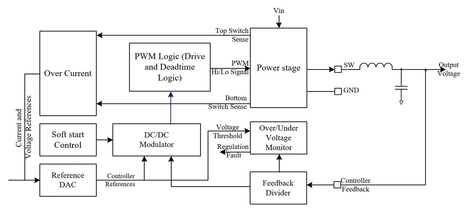
Together, these systems work to form the basics of a power management device, which is shown in Figure 7.
The full design and implementation of each of these circuits depends upon a wide variety of factors specific to the application. In the following sections, we’ll discuss some high-level circuits that make up these blocks, which will allow us to facilitate the completion of our conceptual analysis.
The Safety Analysis
Combining the dependent and failure mode analysis, we can conceptually analyze our architecture and come up with mechanisms and additional architecture enhancements to improve our robustness to hardware failures. While this analysis is not considered to be exhaustive, it will provide some context for a safety manager or product designer evaluating datasheets to compare capabilities.
Internal Rail and Bias Generation
We define the fault models from the DFA, and come up with the following.
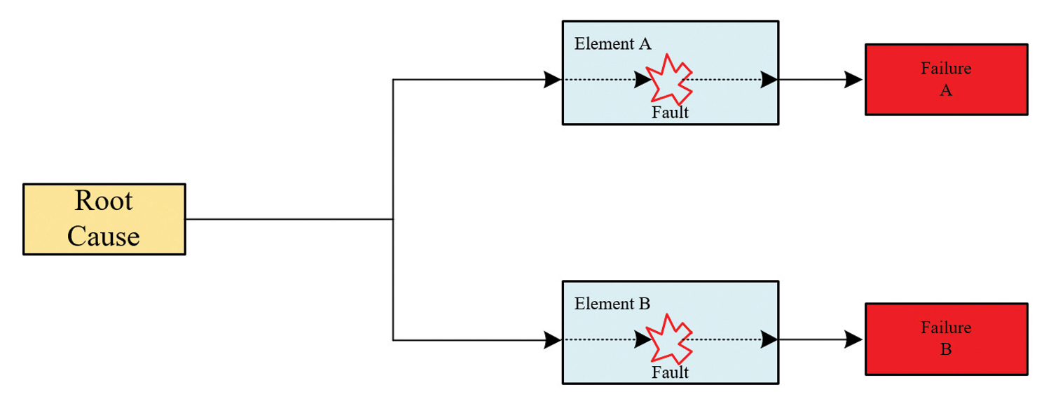
- Common cause faults: Where a singular fault leads to two faults in two separate elements (Figure 8).
- Cascading faults: Where a fault in one element, leads to the fault in another element (Figure 9).
- Drift, due to either component failure or temperature; or
- Oscillation, due to loss of feedback in the voltage generation circuit.
- Distinctly designed bandgaps to prevent both from experiencing the same failure.
- In addition to architectural changes, it is not uncommon to monitor each bandgap against one another, as well as to monitor the source of VCC against a reference over which it has no influence.
The more rigid the safety requirements, the more complex the solution becomes. Now that we’ve addressed dependencies and discussed the implementation of safety mechanisms in the internal bias and power generation section, we turn our attention to the voltage control loop and output switches.
- A voltage control outer loop that utilizes an error amplifier, compensation, reference, and feedback to control the output to a setpoint. In our conceptual architecture, we’ll be utilizing external feedback.
- An inner current loop controller that acts as a quick modifier to the setpoint to compensate for load changes. In our conceptual architecture, we’ll be sensing current through the (integrated) output switches in terms of high and low side current sensing.
- Failure of the output switches by being stuck high or low: This would lead to an irregularity in switching and would cause either an output overvoltage, under voltage, over current, and/or over temperature event due to shoot through or directly connecting the output to either ground or VIN.
- Compensation, which damps the response of the control loop to prevent excessive deviations from the setpoint during a load change, and oscillatory behavior: A potential failure here would be an overvoltage event or oscillatory behavior if the bandwidth of the controller drastically changes.
- A window comparator which measures for over and under voltage on the output; or
- An over current monitor which senses the current through either the high side or low side switch.
Next, we continue with the DFA and automatically clue into the feedback node, which is shared between the regulation and output monitor. If we lose the resistor due to a failure in the resistor divider or if the pin shorts, the device’s regulation will malfunction as the target becomes incorrect, and the monitor runs the risk of not catching it. A DFA leads to the following two criteria:
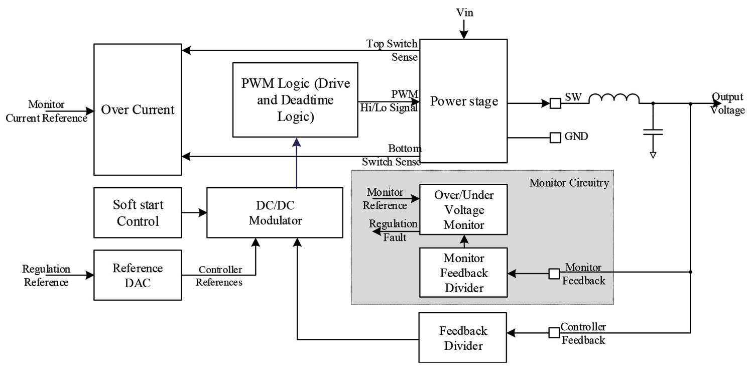
- The device needs to implement two independent sources of feedback to address the dependent failure of the feedback node shorting to another pin or another voltage on the board; and
- This independent source of feedback needs a redundant resistor divider to address the failure mode of any part of the resistor feedback network shorting.
Again, for this reason, it is not uncommon to see a feedback pin and another pin that is used for monitoring. If the feedback resistor is instead internal, then that is redundant and often through a different path. With these additions, we can expand our definition to include an example of what a safety manager or module engineer might see when shopping power parts.
For the last two sections, the design turns its focus to things that are often under the category as monitors instead of the control loop.
- Over current monitors.
- Power on reset detectors.
- Output voltage (over and under voltage) monitoring.
- Internal clock monitoring
Each of these monitors often have the ability to reset/alert downstream components when an irregularity has occurred. Applying our DFA theory again, we notice that the same situation continues to come up, that is, dependencies in the feedback loop and in how we reference the thresholds for the monitors.
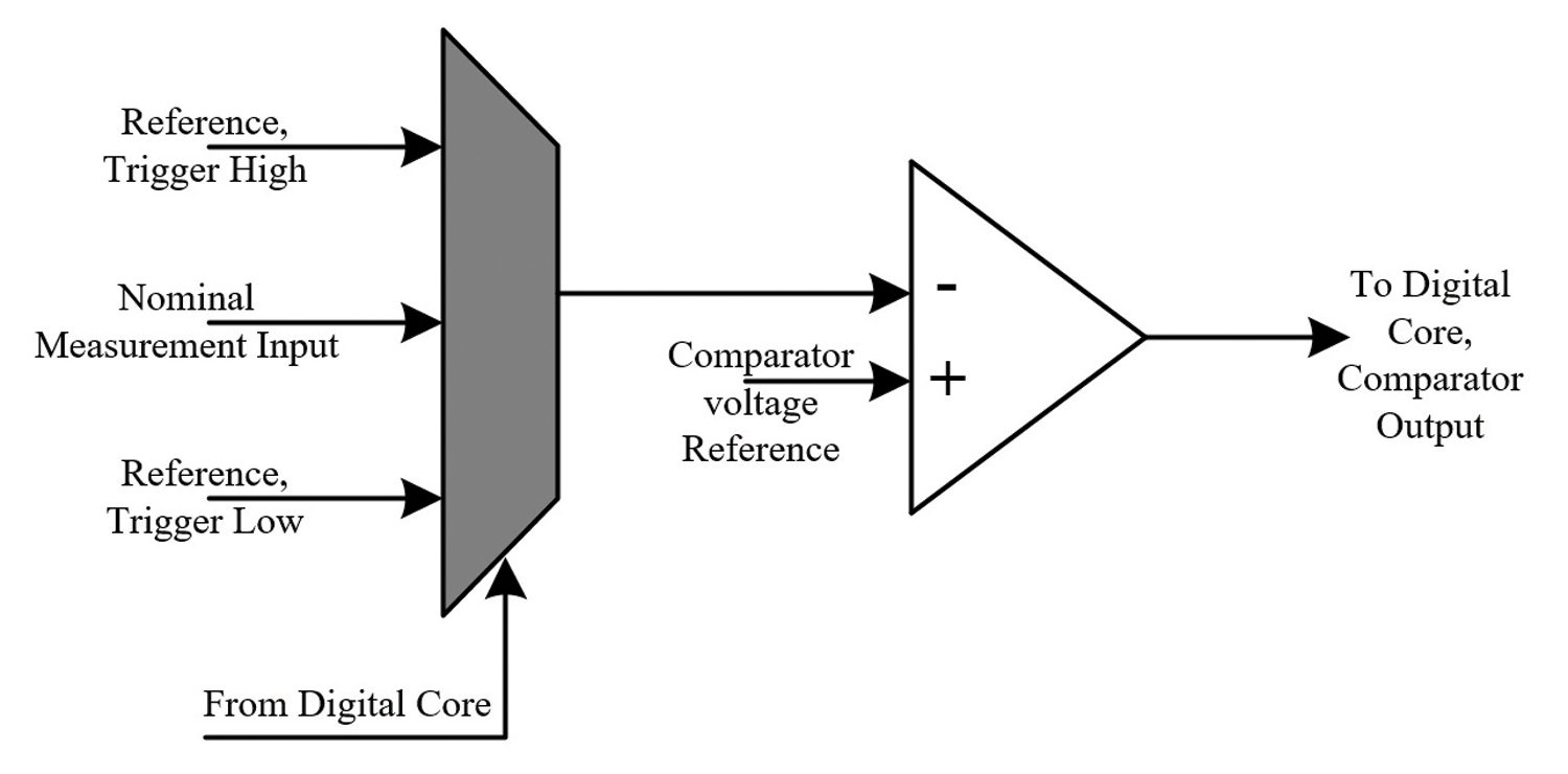
Next, conducting the FMEDA, we apply example failure modes found in ISO 26262 only to the comparator. The faults models here are comparator output stuck at faults (stuck high and low). Of these two faults, stuck low is the more impactful of the two when it comes to monitoring, as the fault occurrence would be missed. In order to increase the device’s ability to detect these stuck low faults, which would cause the device to miss a fault in the event of one occurring, you will often see a term ABIST, an acronym for analog built-in self-test.
The process outlined in Figure 13 allows a brief moment in time for the digital part of the device to take control of the comparator input and force the input above or below the trigger voltage in order to see if the comparator circuit works.
After successful determination, the input control is given back, and it becomes a nominal sensing circuit again. This process takes a moment during startup and is why many datasheets mention some sort of ABIST in their feature section as it is a low impact way of checking for stuck faults.
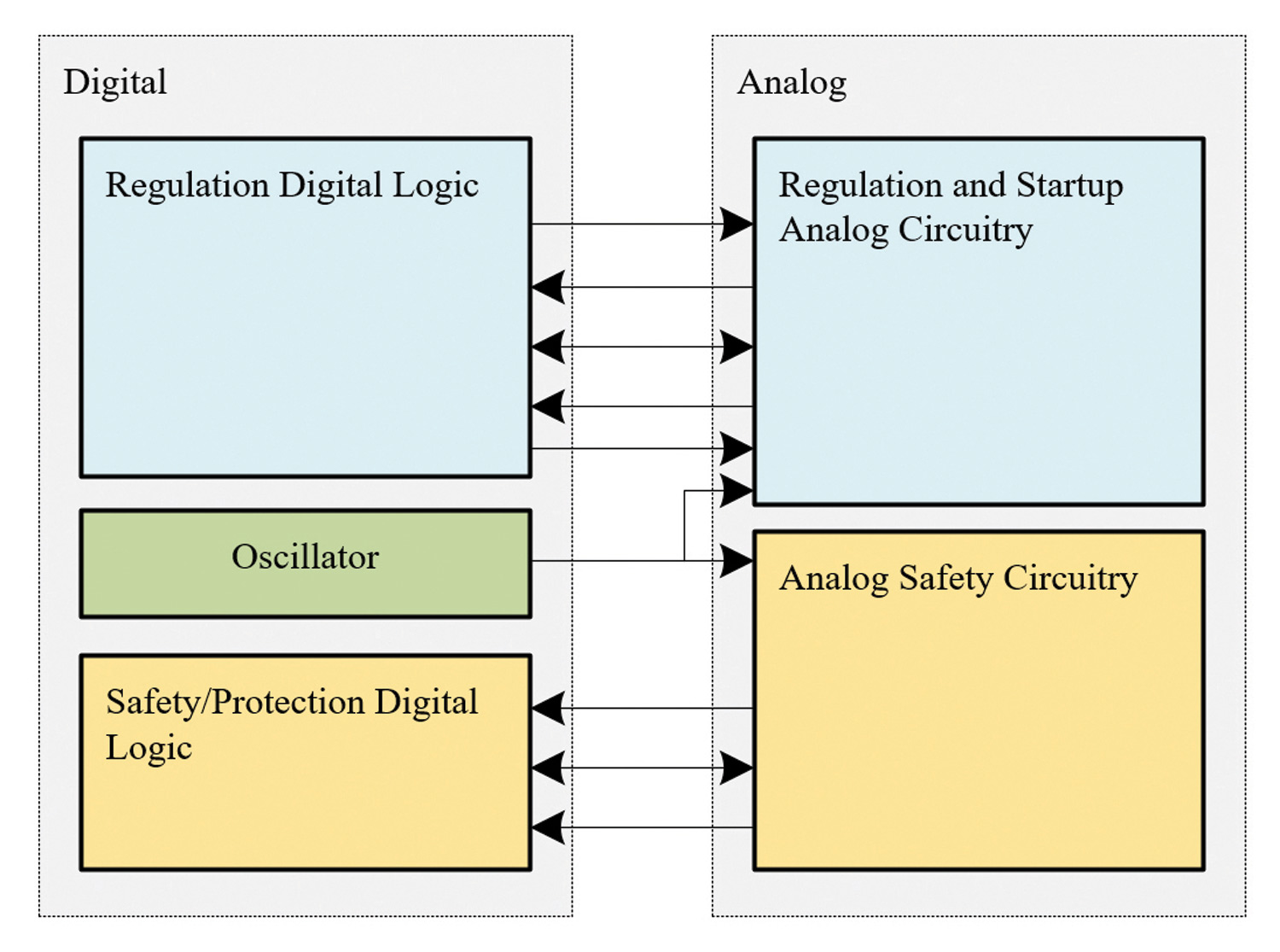
Lastly, we’ll examine the brains, the digital core of a mixed-signal regulator.
- A wide variety of configurations held in fuses and registers;
- A main high-speed oscillator; and
- A serial communications interface- usually I2C or SPI.
This architecture is often preferred to mitigate the possibility of dependencies found through a DFA analysis. In order to better understand the breakup of the digital core, see Figure 14, where the main functions consist of:
- Configuration, often in the terms of runtime configuration registers and one time programmable (OTP) fuses;
- Functional safety decision making, often realized as a state machine; and
- Communication, either implemented as a I2C or SPI controller.
While the list of digital safety mechanisms and design options is vast, it is normal to see the following among the top listed as safety mechanisms in addition to the CRC:
- Redundant logic where necessary;
- Clock monitoring; and
- Logic BISTing (LBIST) which, like the ABIST, checks the digital logic for critical stuck faults.
After addressing each main function of our basic DC/DC buck converter and the random hardware failures associated with these sections, our focus turns on how to evaluate metrics and grade the effectiveness.
The analysis done was qualitative. The process starts with a diagram of interconnections for our power converter and continues by applying industry standard failure modes to each block and reviewing their effects. It continues with the DFA that allows the design team to address dependencies in the architecture, and also allow the device to showcase various safety mechanisms and architectural enhancements that allow for a certain ASIL.
We define the coverage metric as a means for standardizing analysis in a quantitative way across the industry from part to part and manufacturer to manufacturer. This means that if the target for our power converter is an ASIL B system, that would require a specific level of coverage, as opposed to an ASIL D system which requires a higher single point, and latent fault detection coverage. The summary is shown below in Table 2.
And often, you will see comments in the datasheet like “supports applications up to,” which often means that during the analysis, certain assumptions were made that, if followed, would allow for the system to make up for the lack of detection.
Before you begin reviewing your supplier datasheets or before you begin designing, I recommend that you review ISO 26262 as the specification provides an overview of common ways of dealing with faults and provides strategies for low, medium, and high coverage which the industry recognizes. An example is shown in Table 3, but as always, refer to your copy of ISO 26262 for a comprehensive list.
Functional safety is an evolving area of automotive and industrial design, and the right device can be difficult to find since each semiconductor manufacturer presents their product in the best possible way. With each new design comes a new set of safety mechanisms implemented by the design and safety teams, which the marketing team then uses as saleable features. But, without some basic background, this can lead to confusion.
The conceptual analysis presented in this article is meant to give you, the reader, some tools to understanding why ASIL-rated power management devices have the safety features listed in their hardware datasheet. And, in preparing for your next ADAS design, remember that ISO 26262 outlines the tools needed to address both random hardware and systematic design faults, not just high-level digital components but of standard mixed-signal analog/digital designs as well!

