his is the 10th and the final article in a series of articles devoted to the design, test, and EMC emissions evaluation of 1- and 2-layer PCBs that contain AC/DC and/or DC/DC converters and employ different ground techniques [1-9]. The goal of this study was to evaluate the impact of different grounding strategies and the tradeoff with other design constraints that designers often face. In this article, we present the conducted and radiated emissions results performed according to the CFR Title 47, Part 15, Subpart B, Class B.
The board is capable of accepting either an AC or DC input. The AC to DC conversion takes part in Partition A of the board (not drawn to scale). The DC to DC converter in Partition B accepts 24V DC input either from the AC/DC converter in Partition A or from an external source [1]. The AC to DC converter is controlled by a Maxim MAX5022 IC, the DC to DC converter is controlled by MAX17783CATB+.
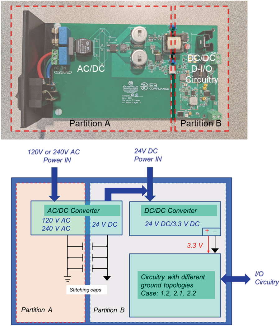
These circuits contained several EMC countermeasures the effectiveness of which are assessed in the previous articles in this series. The AC/DC converter contains an AC input filter, a DC input filter, a slew resistor on the gate of the primary side switching MOSFET, and a snubber on the primary side switching MOSFET. The DC/DC converter contains an input pi filter, a Vishay IHLE electric field shielded switching inductor, and a high frequency output filtering capacitor. The STM32G030F6P6 microcontroller, and MCP7940NT-I/MS real time clock had high frequency decoupling capacitors placed close to the power input pins of the device. The Maxim Integrated MAX31855JASA+ had high frequency decoupling capacitors placed near the power input pins, and a high frequency filtering capacitor across the two pin screw terminal connection for the J-type thermocouple.
Three different PCB topologies were evaluated.
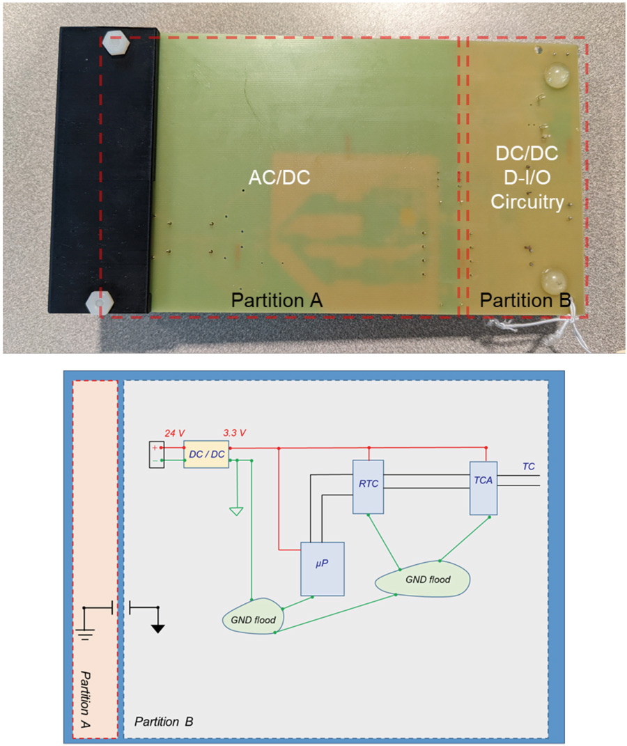
A one-layer board with ground traces and ground floods located only on the top side. The back side of this board is shown in Figure 2.
Next, we evaluated a two-layer board where the bottom layer is a mostly solid ground reference plane with some slots accounting for the need to route signals on the bottom layer. The bottom layer of this board is shown in Figure 3.
And finally, a two-layer board where the bottom layer is a complete ground flood with via stitching to the top-layer ground reference return areas. This is shown in Figure 4.
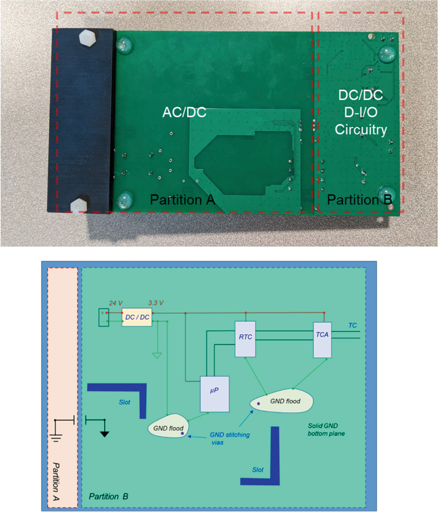
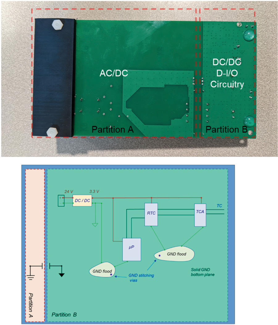
Figure 6 shows the conducted emissions results for a one-layer board.
The conducted emissions results show multiple failures over a wide frequency range.
Figure 7 shows at least 8dB of improvement across most of the 150kHz-30MHz frequency range. We can conclude that introducing a ground reference return (even with slots in it) on the bottom layer significantly improves the conducted emissions performance and results in passing the test.
Figure 8 shows the conducted emissions results for a two-layer board with a solid ground reference return on the bottom layer.
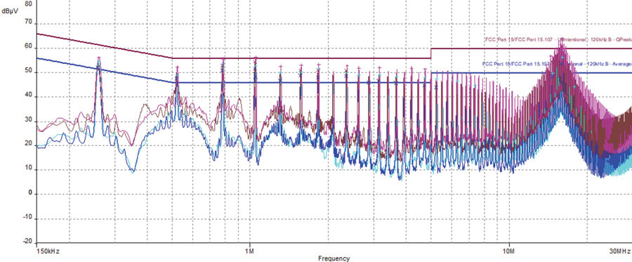
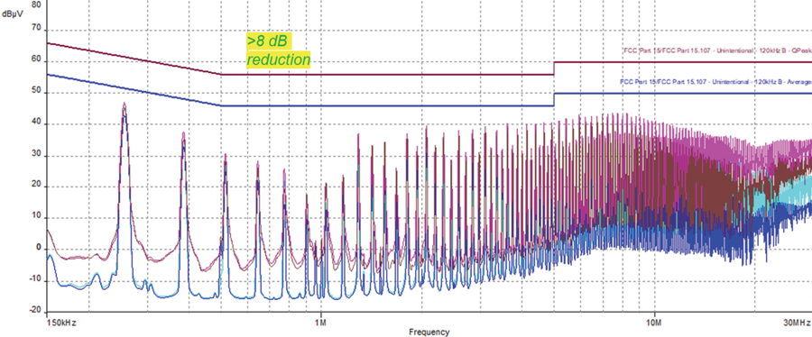
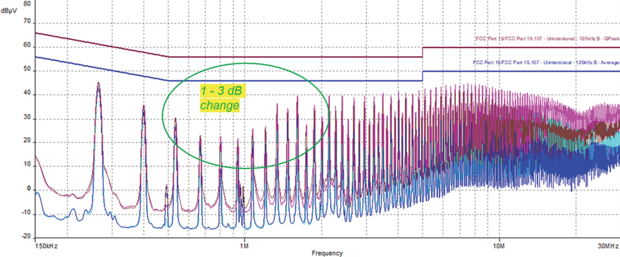
Figure 10 shows the radiated emissions results for a one-layer board.
The single-layer radiated emissions results show multiple broadband failures over the wide frequency range.
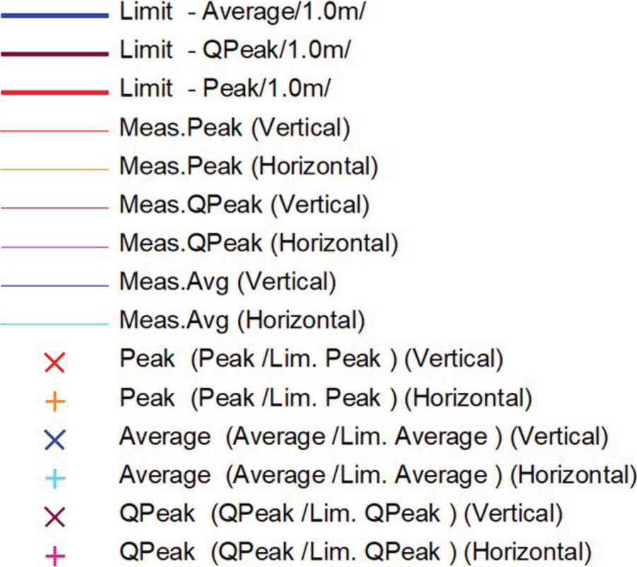
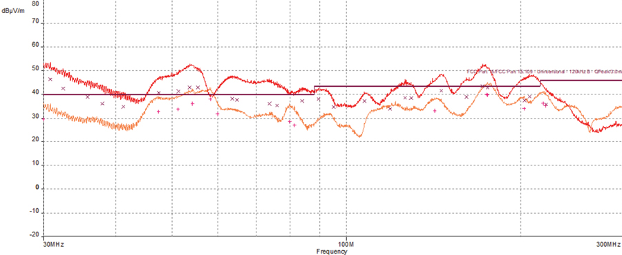
Figure 11 shows that the introduction of a ground reference return, even with slots in it, provides us with a 6-8dB improvement from 30-45MHz, and an improvement of greater than 10dB from 45MHz-240MHz.
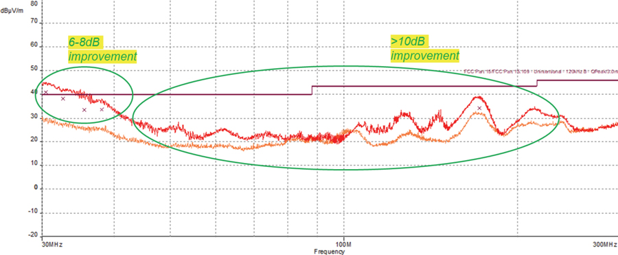
Figure 12 shows the radiated emissions results for a two-layer board with solid ground reference return.
- PCB layout can have a dramatic effect on RF emissions performance
- The ground reference return in the power converter designs used should be:
- Filled on adjacent layers to the extent possible to provide a good reference return
- Connected as direct and low impedance as possible between input filtering reference to output filter reference
- Stitched between layers to improve the reference return path
- It is recommended to fill with ground reference beneath switching magnetics when possible (eg. Isolation issues, efficiency issues allow it)
- Lower frequency emissions failures in conducted and radiated emissions can be addressed by ensuring good input and output filtering
- Mid to high frequency emissions failures in conducted and radiated emissions can be improved through the use of snubber circuits, gate drive slewing, good decoupling, and PCB or inductor shielding
- In isolated switching supplies, stitching capacitance is important to evaluate and tune to optimize emissions performance without violating any isolation requirements
- Adamczyk, B., Mee, S., Koeller, N, “Evaluation of EMC Emissions and Ground Techniques on 1- and 2-layer PCBs with Power Converters – Part 1: Top‑Level Description of the Design Problem,” In Compliance Magazine, May 2021.
- Adamczyk, B., Mee, S., Koeller, N, “Evaluation of EMC Emissions and Ground Techniques on 1- and 2-layer PCBs with Power Converters – Part 2: DC/DC Converter Design with EMC Considerations,” In Compliance Magazine, June 2021.
- Adamczyk, B., Mee, S., Koeller, N, “Evaluation of EMC Emissions and Ground Techniques on 1- and 2-layer PCBs with Power Converters – Part 3: DC/DC Converter – Baseline EMC Emissions Evaluations,” In Compliance Magazine, July 2021.
- Adamczyk, B., Mee, S., Koeller, N, “Evaluation of EMC Emissions and Ground Techniques on 1- and 2-layer PCBs with Power Converters – Part 4: DC/DC Converter – EMC Countermeasures- Radiated Emissions Results,” In Compliance Magazine, August 2021.
- Adamczyk, B., Mee, S., Koeller, N, “Evaluation of EMC Emissions and Ground Techniques on 1- and 2-layer PCBs with Power Converters – Part 5: DC/DC Converter – EMC Countermeasures- Conducted Emissions Results,” In Compliance Magazine, October 2021.
- Adamczyk, B., Mee, S., Koeller, N, “Evaluation of EMC Emissions and Ground Techniques on 1- and 2-layer PCBs with Power Converters – Part 6: PCB Layout Considerations,” In Compliance Magazine, November 2021.
- Adamczyk, B., Mee, S., Koeller, N, “Evaluation of EMC Emissions and Ground Techniques on 1- and 2-layer PCBs with Power Converters – Part 7: AC/DC Converter Design with EMC Considerations,” In Compliance Magazine, December 2021.
- Adamczyk, B., Mee, S., Koeller, N, “Evaluation of EMC Emissions and Ground Techniques on 1- and 2-layer PCBs with Power Converters – Part 8: Baseline EMC Emissions Evaluation,” In Compliance Magazine, January 2022.
- Adamczyk, B., Mee, S., Koeller, N, “Evaluation of EMC Emissions and Ground Techniques on 1- and 2-layer PCBs with Power Converters – Part 9: EMC Countermeasures – Conducted and Radiated Emissions Results,” In Compliance Magazine, February 2022.