
s a technical consultant, I have seen various new technologies implemented in both new and old applications. In the semiconductor industry, WBG devices such as SiC and GaN transistors have been gaining attention due to their small size, fast speed, and better thermal performance. The introduction of these new semiconductors into the consumer market came after a series of military and other commercial applications of the technology in everything from electric vehicles to radar systems.
GaN devices have enabled a much better form factor for product design than their silicon counterparts. As they become cheaper and more available, it is expected that we will see them widely adopted in power-switching modules worldwide.
Technically speaking, GaN semiconductors are high-electron-mobility transistors (HEMTs), meaning they do not have the doped region in a PN junction like MOSFETs. This enables faster electron flow, hence higher switching speed. Because HEMTs do not have the PN structure, they also do not have a body diode. This can have a great impact in applications such as motor drives, where we can now switch on the HEMT for freewheeling rather than relying on the body diode.
From the EMC perspective, this feature can be useful as, traditionally, EMI issues associated with the reverse recovery charge of a body diode during deadtime can be a problem [1]. To fix the issues, engineers often place a Schottky diode in parallel with the MOSFET as Schottky diodes switch faster and do not have a reverse recovery charge effect [1]. Now that the switching speed of a GaN is faster than a Schottky diode, it does not have a reverse recovery charge effect either. The HEMT has a “quasi diode” mode in the deadtime region, and we need to control the deadtime well.
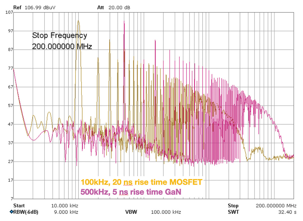
But new technology often presents a double-edged sword. The most significant advantage of a GaN device (superfast switching, say 100V/ns) also brings a challenge for controlling EMI. As we all know, the faster the switching action (i.e., defined by the rise time), the harder it is to contain EMI, especially above the frequency of 1/πt, where t is the rise/fall time of a switching event. This can be seen in Figure 1.
In other cases, engineers have chosen to use silicon MOSFETs based on trade-off calculations in the design. For instance, if using a WBG device results in requiring an additional filter to pass EMC, it is not a good idea as the filter would add cost and weight. But, given a good product design with EMC consideration in the design stage, it is believed that a WBG device should be the device of choice, supporting efforts to achieve the best possible product form factor and resulting in higher performance and lower cost. This can already be seen in the laptop/mobile phone charger market, where GaN chargers have started dominating the market.
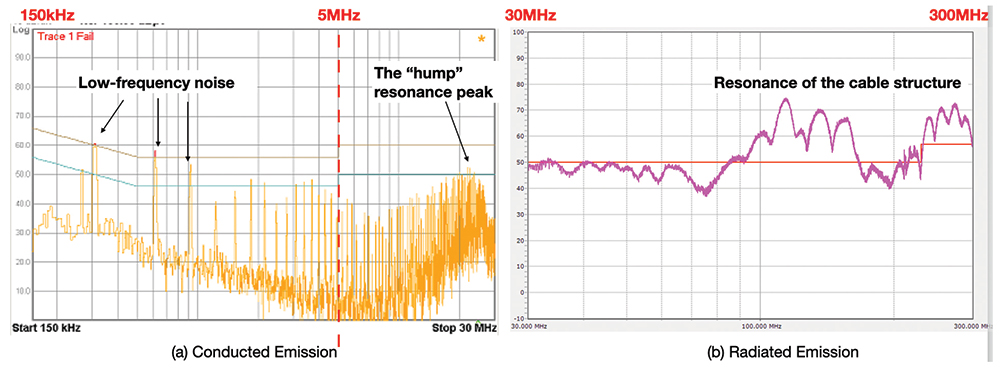
- 150 kHz to 5 MHz range: This constitutes the low-frequency conducted emission test range. Here, strong electromagnetic noise is generated due to the hard switching event, typically associated with the switching frequency. While most of the noise in this range is differential mode, in high-power applications with WBG devices it can also be common mode dominant, as demonstrated in [2].
- 5 MHz to 30 MHz range: In this range, common mode noise becomes prevalent. It’s important to note the presence of a “hump” in this region, caused by structural resonance introduced by the test setup. When the device under test experiences a hard switching event, it exhibits a resonance peak in the test results [3]. The energy level is determined by the rise time of the switching event in the 10s of MHz frequency range.
- 30 MHz to 300 MHz range: This is the far‑field radiated emission test range. In this frequency range, it is most likely that the failure mode is caused by the cable acting as an efficient antenna, leading to radiated emission issues. Beyond 300 MHz, radiated emission failures caused by power electronic devices become less common.
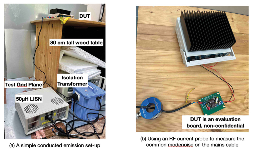
- Expensive test equipment: With faster switching frequencies and shorter rise times, an oscilloscope with a bandwidth of at least 500 MHz is necessary to accurately measure the rise time. This means investing in higher-end and more expensive testing instruments. It’s worth mentioning that a 500 MHz bandwidth oscilloscope proves more advantageous for electronics development tasks than for EMC purposes (although a higher bandwidth always helps). This is particularly beneficial as engineers frequently require accurate rise time measurements to calculate switching losses and ensure overall system efficiency.
- Challenges with measuring: Using a standard 500 MHz passive probe might not yield the most accurate results when measuring the switching events of WBG devices. Probe resonance and ground lead issues can introduce common impedance-induced errors, leading to inaccuracies in the measurements [4]. For precise measurements, a high-end optical isolated differential probe is preferred, but the cost of such a probe alone can easily exceed $10,000.
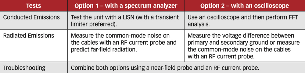
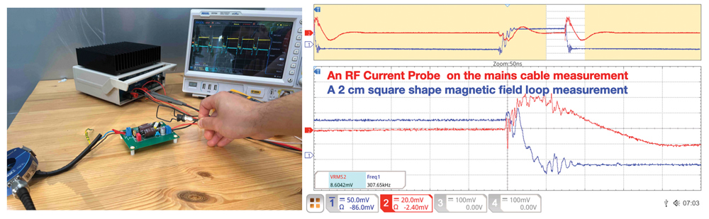
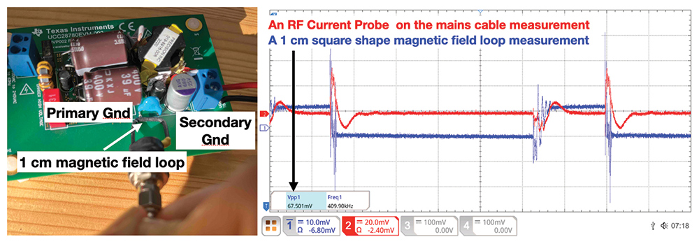
Common-mode noise currents have the ability to flow between an isolated output ground (often referred to as 0V_gnd or secondary ground) and the power supply input ground (commonly known as HV- or primary ground). These currents can attain considerable amplitudes, leading to Ldi/dt voltage drops between the grounds. Additionally, when both input and outputs are wire-connected to the source and the load, these wires function as efficient dipole antennas.
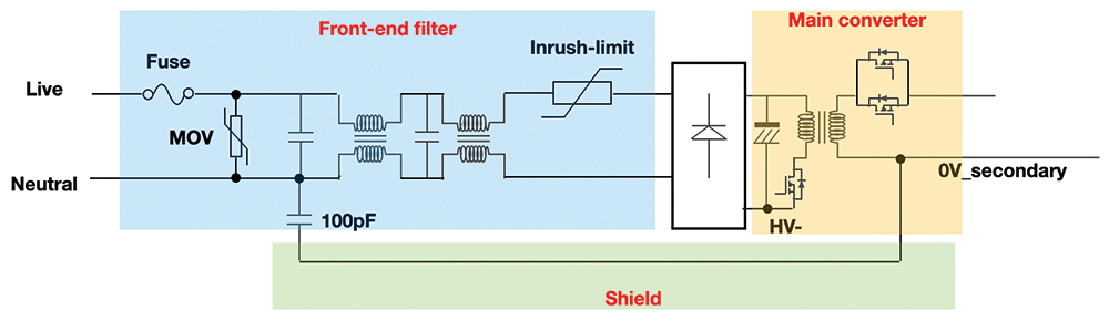
For chargers below 100 watts, the most popular topology is an active-clamped flyback converter. On the other hand, for chargers above 100W, the design of choice often involves an LLC with a PFC converter. Despite the topology specifics, we can generalize this type of isolated power supply as depicted in Figure 6.
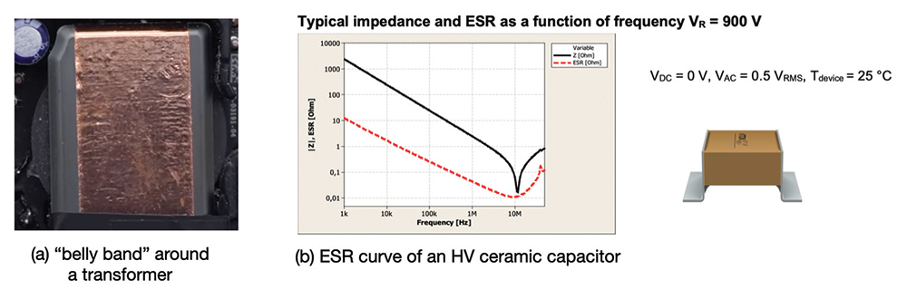
- Transformer: Whether designed in-house or bought off-the-shelf, the key consideration for EMC is the parasitic capacitance introduced by the windings. Minimizing the parasitic capacitance is essential, preferably aiming for it to be at least ten times smaller than the capacitance value of the Y-class capacitors used in such systems. Detailed design techniques for various converters are beyond the scope of this article. Another useful technique is to use a copper sheet (nicknamed “belly band”) around the transformer (see Figure 7(a) below). This sheet acts as a “flux cancellation” plane (as the induced eddy current forms a magnetic flux which is opposite to the transformer flux), and there is no need to “ground” the sheet, easing the manufacturing process.
- Grounds: Both the primary and secondary grounds should have substantial copper areas on the PCB, preferably placed on the same side, with minimal distance between them (HV safety permitted). A Y-class capacitor is essential to join the two grounds, providing a low-impedance path for common mode currents. However, the capacitance value is limited by the maximum leakage current requirements.
- DC link capacitors: Achieving a low-impedance DC link is crucial, and this is typically accomplished through a combination of electrolytic capacitors and ceramic caps. Film caps are not suitable for the DC link in this application due to cost and size requirements. There have been discussions within some R&D projects regarding the replacement of electrolytic capacitors with high-capacitance ceramic capacitors to achieve a higher form factor. However, this proposition faces challenges currently:
- Too many ceramic capacitors in parallel can lead to excessive and uncontrollable system resonance; and
- Datasheets suggest that ceramic capacitors can exhibit very high equivalent series resistance (ESR) in the very low-frequency range, which adversely affects the performance of low-order harmonics if they replace electrolytic caps (see Figure 7 (b)).
If not designed properly, significant ringing can be observed on the primary side switching with a GaN/SiC device. The ringing frequency depends on the stray inductance in the design (often the transformer leakage inductance) and the parasitic capacitance of the switching device. To reduce this ringing, considerable effort should be focused on the following approaches:
- Implementing an RC snubber circuit;
- Placing DC link decoupling capacitors close to the switch; and
- Optimizing transformer design and implementing a shield over the transformer.
It is worth noting that a control feature such as ZVS can sometimes introduce noise in light load conditions. It is the design engineer’s job to check the EMI performance in all operation modes (light and heavy loads).
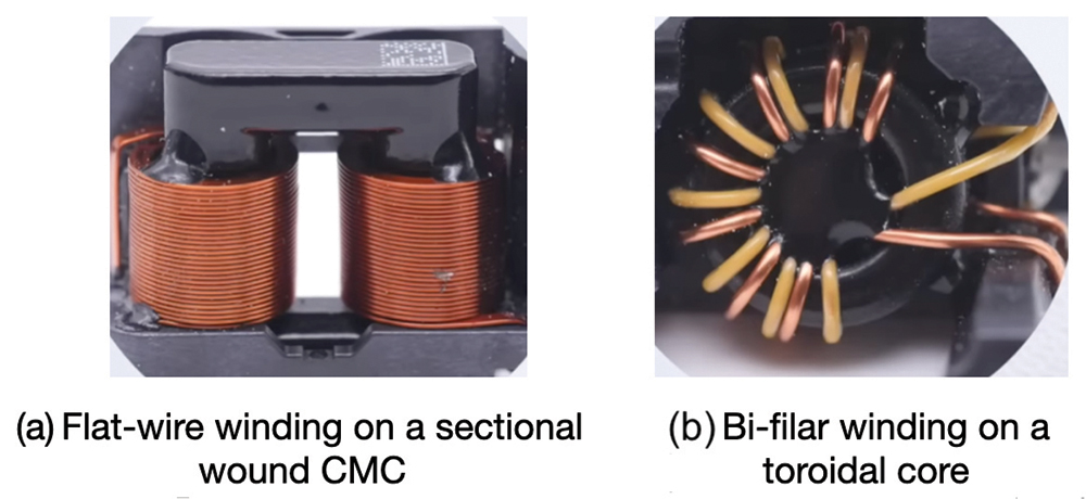
Employing a two-stage filter is critical. The low-frequency conducted emission failures seen in the evaluation board (in Figure 2) occur due to the sole use of a one-stage filter. The capacitors used in the front-end filter should be film-type. For a more effective solution, a typical two-stage filter should incorporate two types of common mode chokes as key magnetic components:
- A sectional wound high inductance common mode choke to suppress noise between 150 kHz and 5 MHz; and
- A bi-filar wound, low inductance common mode choke for higher frequency noise suppression.
On the other hand, the bifilar wound common mode choke, designed for high‑frequency filtering, cannot have too many turns. Its bifilar winding configuration wound on a toroidal core offers minimum leakage inductance (close to zero), making it ideal for high common mode noise suppression. Figure 8 illustrates both types of common mode chokes used in a charger.
By strategically combining these two-stage filters with different choke designs, a comprehensive and effective front-end filter can be achieved, ensuring successful EMC performance for WBG-based devices.
- When wrapped around a transformer, it cancels some of the magnetic field by inducing eddy currents on the metal sheet; and
- It provides electrical field shielding when properly “grounded.” For manufacturing convenience, the ideal “grounding” point should be 0V_ground on the secondary side of the transformer. The other grounding point should be the earth point (if present). In the case of safety Class II products, where user protection from electric shock is achieved through two levels of insulation (double or reinforced) without the need for earthing, the shield is often connected to the neutral line via a small Y-class capacitor, as depicted in Figure 6.
- M. Zhang, “Demystifying EMC in an Electric Vehicle’s Drive Unit,” Interference Technology.
https://interferencetechnology.com/demystifying-emc-in-an-electric-vehicles-drive-unit - M. Zhang, “Troubleshooting Low-Frequency Common Mode Emissions,” Signal Integrity Journal.
https://www.signalintegrityjournal.com/articles/2965-troubleshooting-low-frequency-common-mode-emissions - T. Williams, EMC for Product Designers, Fifth Edition, Newnes, 2017.
- D. Smith, High Frequency Measurements and Noise in Electronic Circuits, Springer, 1993.
- M. Zhang, “In-Situ Radiated Emission Testing of Large Systems Installations,” In Compliance Magazine, July 2023.
https://incompliancemag.com/article/in-situ-radiated-emission-testing-of-large-systems-installations - S. Sandler, “How Fast is the Switching Speed of a GaN Switch?” Signal Integrity Journal.
https://www.signalintegrityjournal.com/blogs/15-extreme-measurements/post/2309-how-fast-is-the-switching-speed-of-a-gan-switch
