or decades, Moore’s law has been driven by the downscaling of transistor dimensions on silicon. When reaching the ultra-advanced integrated circuit (IC) fabrication technologies in the single-digit nm regime (currently 5 nm CMOS is in volume ramp) there is little headroom left, and a different path of packing more functionality into an even smaller volume at the lowest power and cost has to be taken. 3D and 2.5D IC packaging technologies have become primary candidates to serve this purpose [1]. Both packaging technologies, which are often also referred to as ‘heterogenous integration’, have reached the maturity for volume production and can already be found in products.
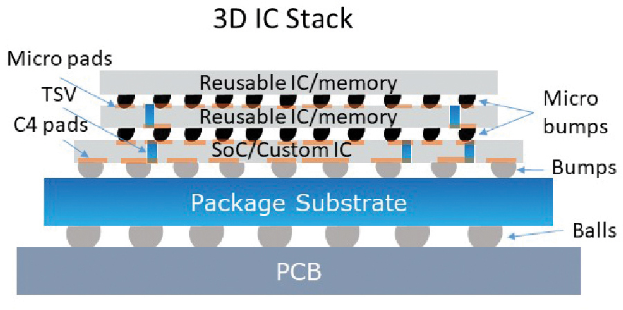
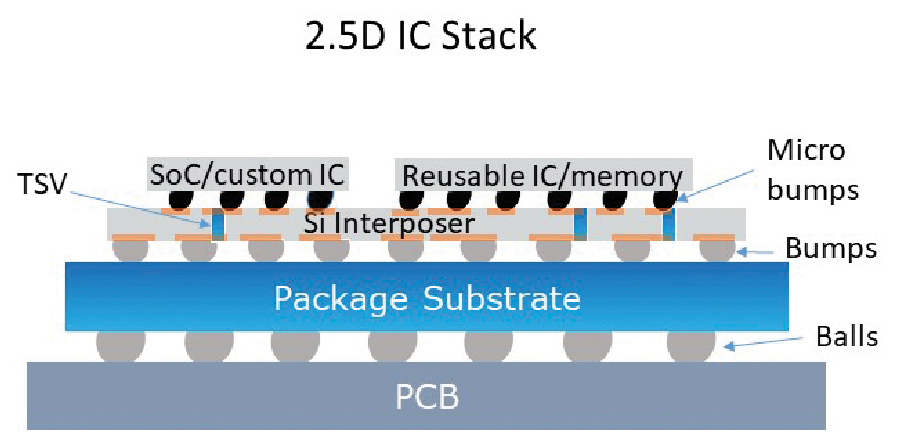
A valid question to ask is what is 3D or even 2.5D packaging about? 3D packaging means to stack dies of silicon on top of each other and contact them in large numbers by die-to-die connections (see Figure 1). Today thousands of interconnects are running between a bottom die and a top die. This is predicted to grow into the tens of thousands to millions of interconnects per square millimeter of die area. One essential step in the process is to use so-called through silicon vias (TSVs) to route power and signals from the bottom side to the top side of a die. 2.5D packaging in contrast describes the assembly of silicon dies side-by-side atop an interposer substrate, which serves as a carrier on which the routing lines/connectivity between the dies are implemented (Figure 2).
At the same time, these packaging methods also allow the optimization of the ESD protection design for package balls. Some of the area-consuming IO ESD protection circuits on expensive 5 nm CMOS technology dies might move to the interposer processed in a much less expensive technology. The new ESD protection architectures and the management of the models and parameters for dies manufactured in different technologies and incorporated into one ESD protection network will pose a challenge for ESD and latch-up verification tools and methods. It is definitely not a new challenge, but one that needs to be tackled soon to better address 3D package designs.
- Semiconductor Industry Association, International Technology Roadmap for Semiconductors (ITRS), 2015.
- Industry Council on ESD Target Levels, White Paper 2, A Case for Lowering Component Level CDM ESD Specifications and Requirements, Rev. 2.0, 2011.
- EOS/ESD Association, Inc. Electrostatic Discharge (ESD) Technology Roadmap, 2020.