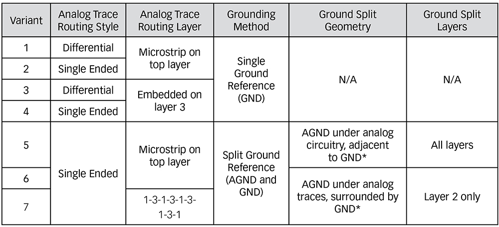
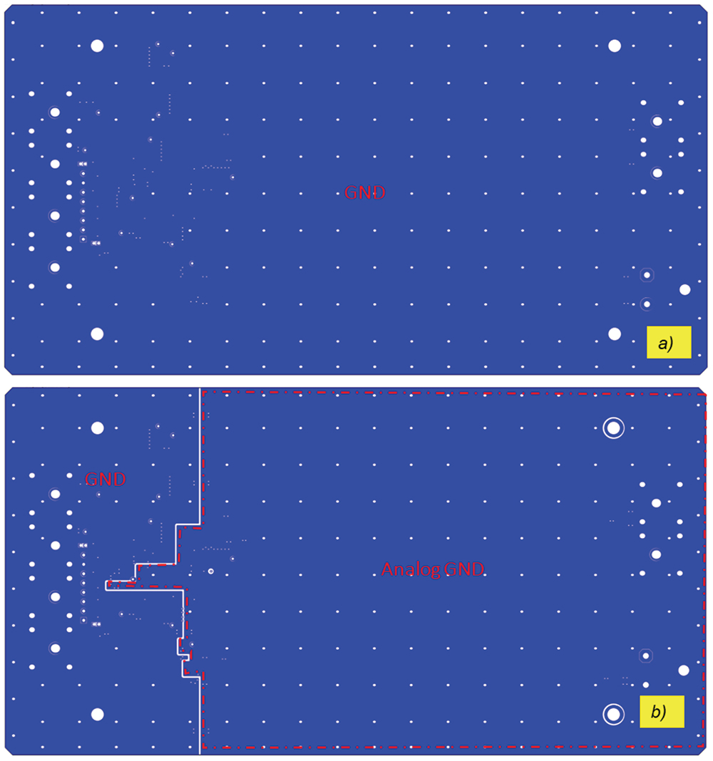
his is the first of three articles devoted to the design, test, and electromagnetic compatibility (EMC) immunity evaluation of multilayer PCBs containing analog circuitry. In this study, there are seven design variants that all contain a similar schematic but implement different PCB layout techniques.
All variants were equipped with an analog voltage measurement along with a temperature measurement [1]. Non-conductive and metallic enclosures were evaluated for cases where the design options showed susceptibility issues. Testing was performed according to the ISO11452-11 Radiated Immunity Reverberation Method standard from 200MHz – 1GHz up to 100V/m and ISO11452-4 Bulk Current Injection from 1MHz – 400MHz up to severity level 4. The analog readings were monitored during RF immunity testing to determine the performance of the various design options.
In this introductory article, we present a top-level block diagram description of the design problem under research. The subsequent articles will be devoted to the RF immunity performance of the PCB assemblies.
Many electronic devices use sensors to monitor their environment, interpreting analog signals and quantizing them into discrete values for digital use. For example, temperature and battery voltage are commonly measured in a variety of applications, which is the case in this study.
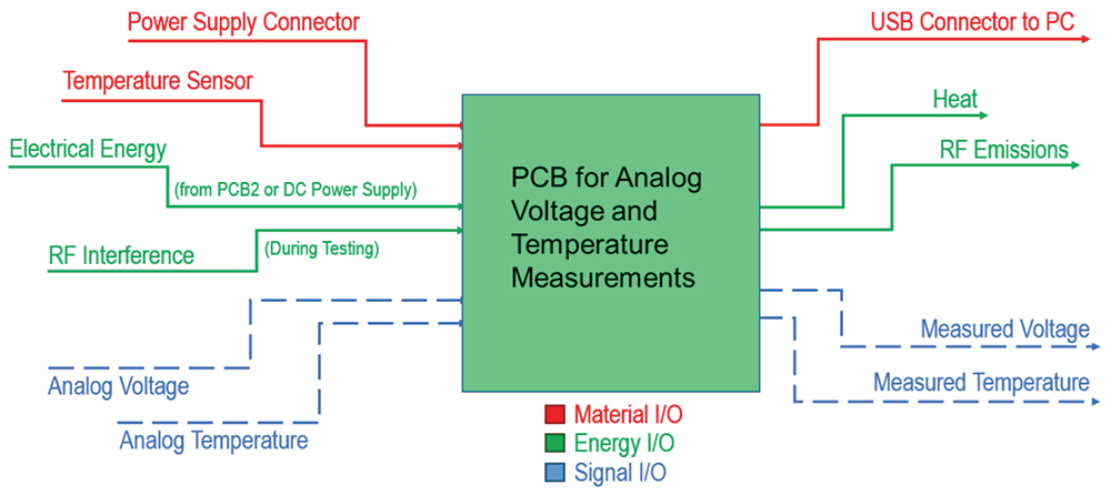
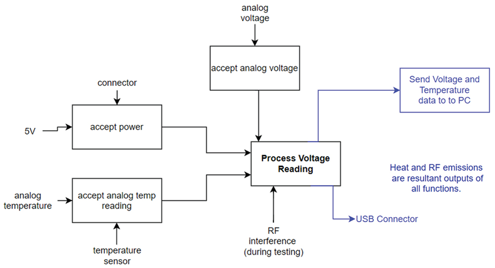
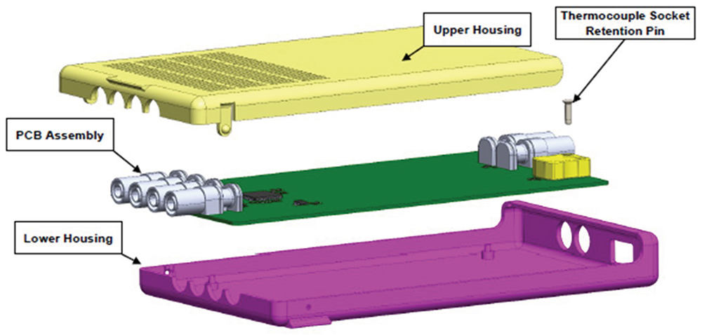
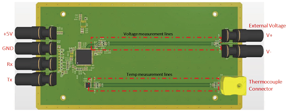
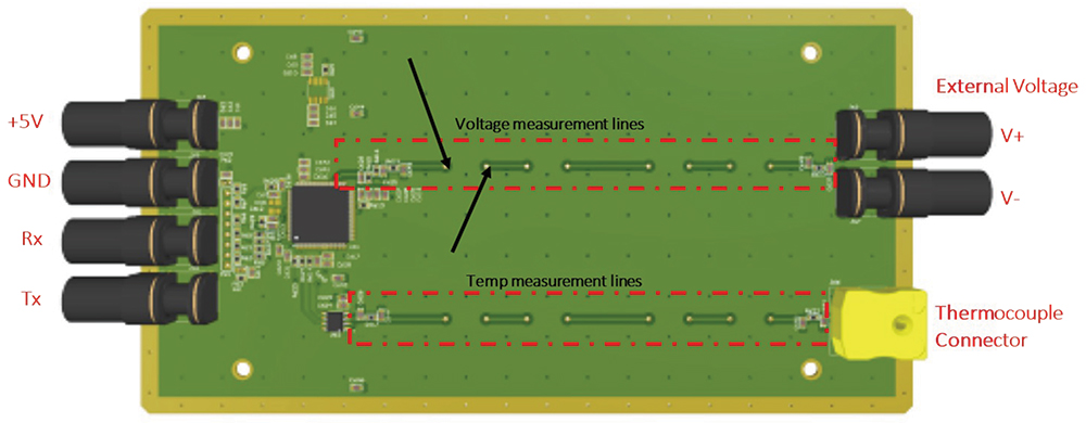
For the purposes of this study, we focused on the electrical interfaces. A 5VDC supply was provided to power the PCB. A separate 12VDC power supply was provided for the analog voltage measurement. Additionally, a thermocouple was connected to the analog measurement port. In response, the PCB provided the measured values of Voltage & Temperature over UART back to the PC through a fiber optic interface. The functional structure of the measurements is shown in Figure 2.
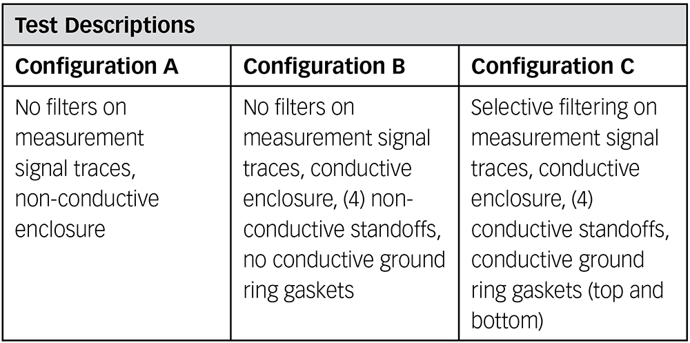
All seven variants were tested using Configuration A. The three variants which exhibited the weakest RF immunity performance were re-tested in the frequency bands where the failures occurred, using Configuration B (variants 1,5,6). Finally, the worst performing variant from the second round of testing (Configuration B) was re-tested using Configuration C (variant 1), again in the frequency bands where the failures occurred.
- Baatar, B., Costantino, C., Morey, R., Muldowney, C., “EMC PCB Design Study”, GVSU senior project sponsored by E3 Compliance, LLC.