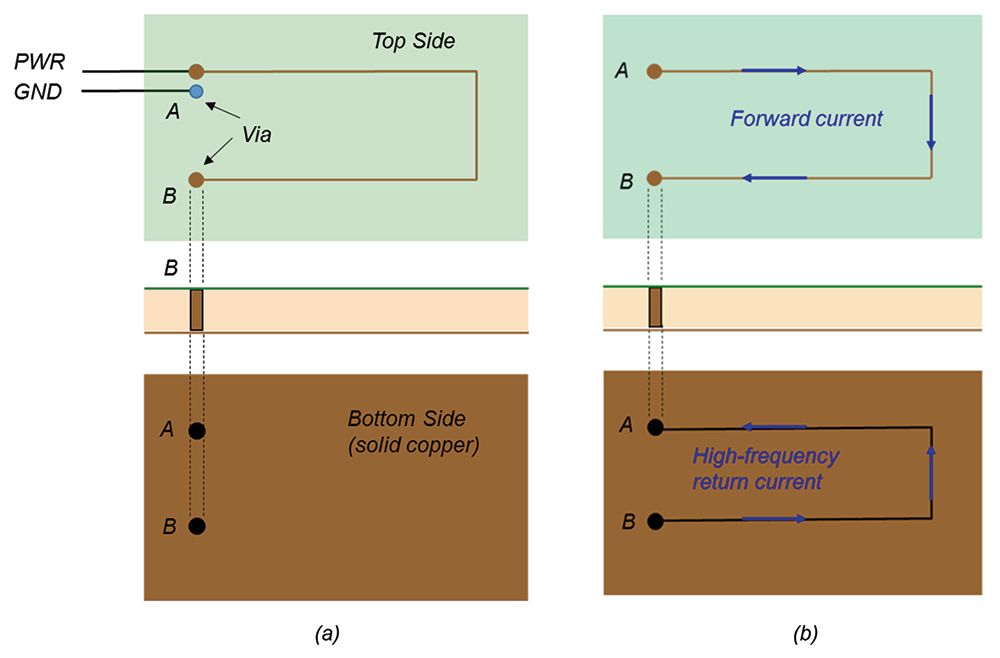
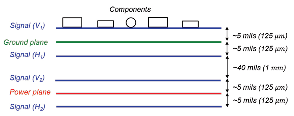
n [1] the return path of high-frequency current was discussed for a two-layer PCB configuration shown in Figure 1a.
It was shown that at high frequencies the return current takes the path of least inductance, which is directly underneath the top trace, because this represents the smallest loop area (smallest impedance). This is shown in Figure 1b.
This article discusses the distribution of a PCB return current underneath top trace for the microstrip configuration. Next month’s article will discuss the distribution for the stripline configurations.
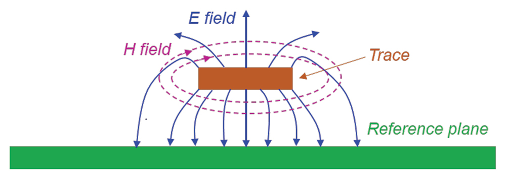
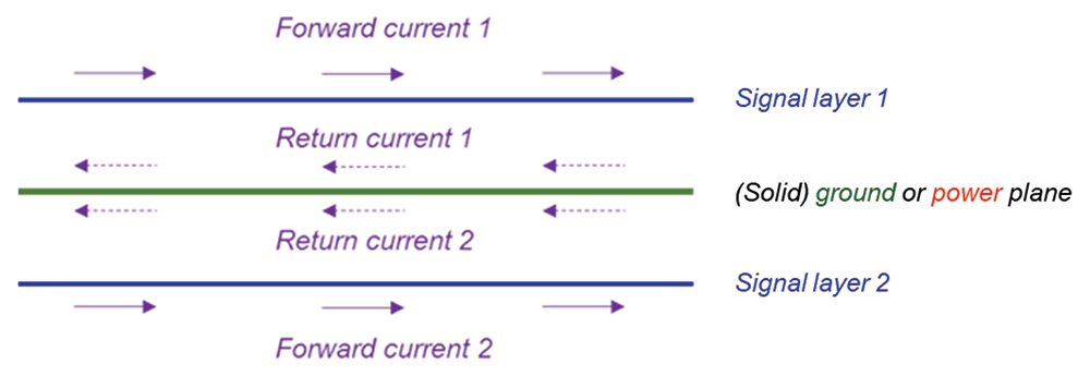
Figure 3 shows a single trace on a signal layer carrying a forward current and the associated fields.
This seems to contradict what we have learned in a basic circuit course. In a “classical” circuit course we always assumed that the current flows out of the positive terminal of the source, flows along the forward path, through the load, and returns to the source on the return (ground) path (conductor or plane).
This is true for pure DC currents where we model the current flow as moving charges along the conductor, flowing with a drift velocity proportional to the voltage of the source. We often ignore the drift velocity and assume that there is no time delay in the current flow and the voltages and currents appear instantaneously everywhere in the circuit when the source is connected to it.
Pure AC current (regardless of its frequency) does not involve the charges moving along a conductor; it is modeled as the charges oscillating back and forth (with respect to their original position) as the polarity of the source changes. This ac model is valid for the functional, i.e., intentional ac currents. When analyzing such circuits, we still assume that the current flows from the positive terminal of the source, along the forward conductor to the load, and returns to the source along the return (ground) path (conductor or a plane). And again, we often ignore the time delay.
Now, the situation is quite different for high-frequency noise currents. Actually, for any-frequency noise currents, but we usually ignore the low-frequency noise and focus on high-frequency noise currents. These high-frequency noise currents, (created for instance, during the switching of the DC voltage levels) are superimposed on the existing functional DC or AC currents. In understanding their impact, it helps to think of them as the electromagnetic waves traveling on the surface of the conductor. These waves disturb the functional behavior of the charges moving in a conductor, regardless of what DC potential the conductor is at! These high-frequency noise waves (current) will “flow” on any conducting surface, regardless of whether it is a ground or power plane!
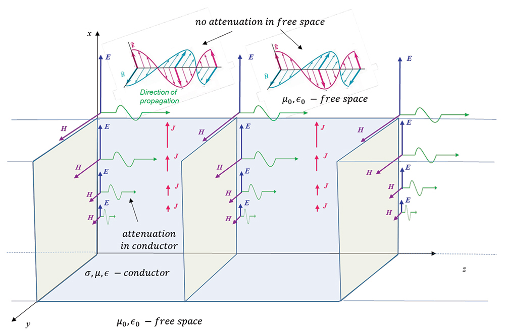
Figure 8 shows the fields and the current density inside the current carrying conductor (see [3] for more details).
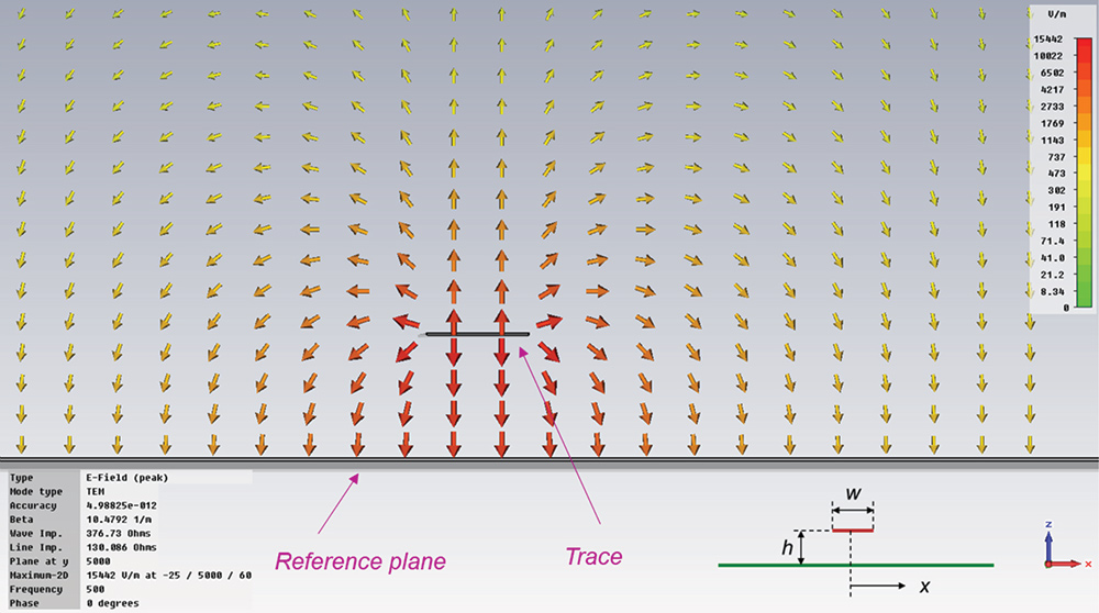
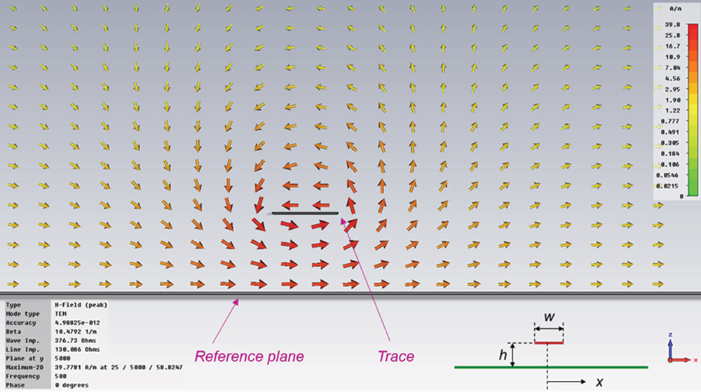
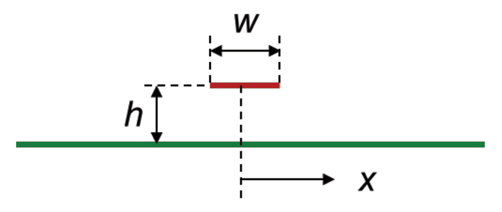
Let’s turn our attention to the return current distribution in the reference plane underneath the forward trace. Consider the microstrip line geometry shown in Figure 10, where the trace of width w is at a height h above a reference plane; x is the distance from the center of the trace.


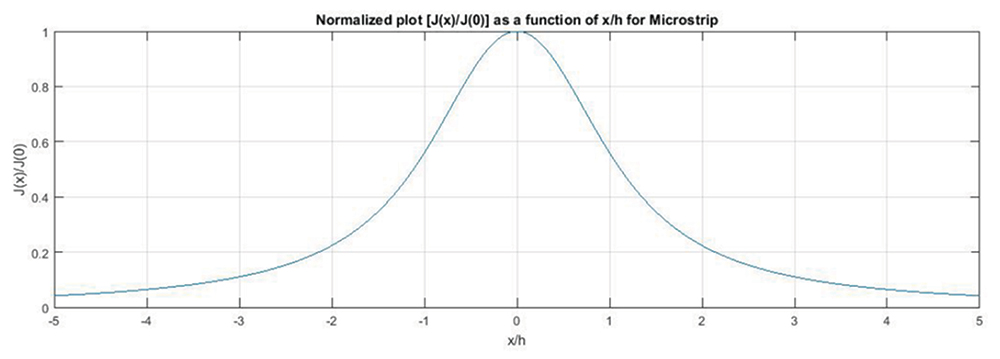
Observations: 1) Majority of the return current flows relatively close to the center of the trace. 2) as the distance from the center increases, the curve flattens. Therefore, there is still some return current beyond the distance ±5x/h from the center.
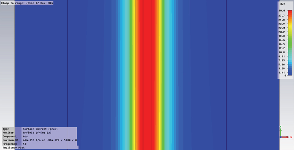
Figure 12 shows the CST Studio simulation of the current density underneath the trace.
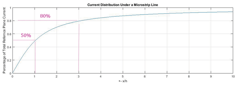
Figure 13 shows the % of the total microstrip return current contained in the portion of the plane between ±x⁄h of the centerline of the trace.
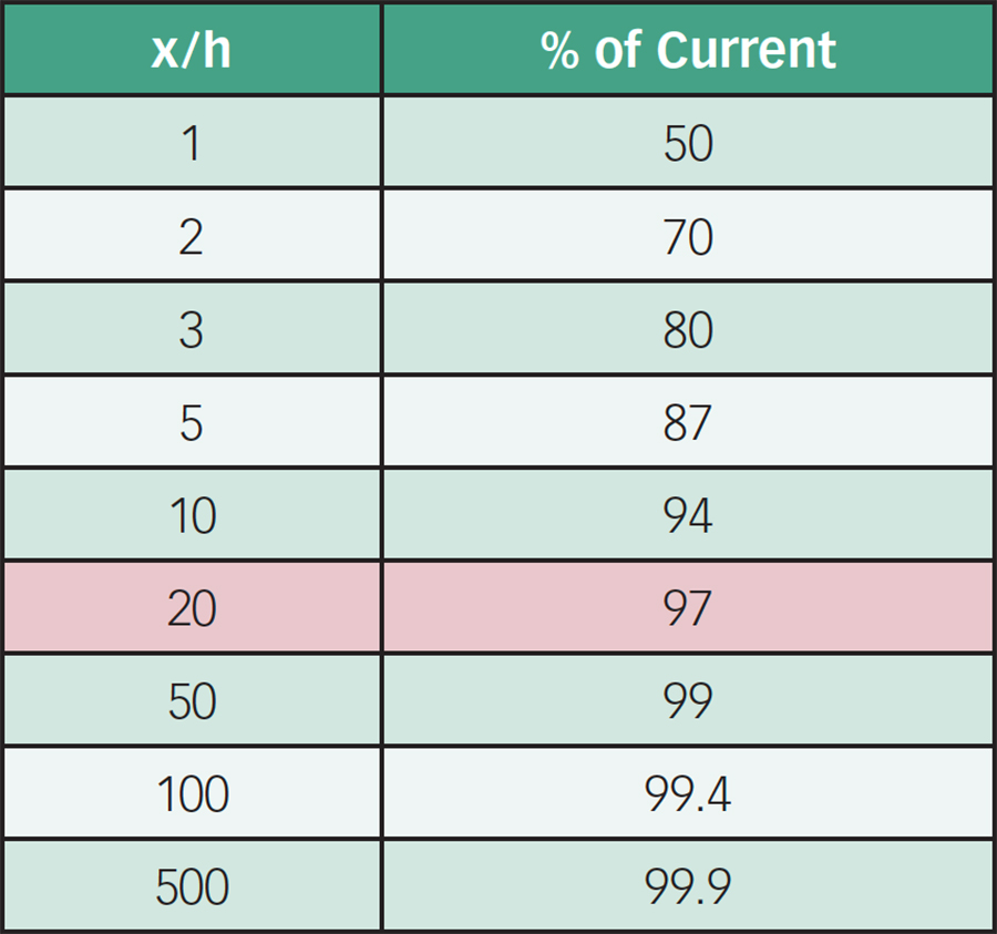
Table 1 shows more detailed results for other distances from the centerline underneath the trace [x].
The highlighted row in Table 1 shows that if a microstrip trace is located 10 mils above a reference plane, then 97% of the return current will flow in the portion of the plane that is 200 mils to the left and right of the trace centerline.
- Bogdan Adamczyk, “Common-Mode Current Creation and Suppression,” In Compliance Magazine, August 2019.
- Scott Piper, CST Microwave Studio Simulations, Gentex Corporation, 2012.
- Bogdan Adamczyk, “Skin Depth in Good Conductors,” In Compliance Magazine, February 2020.
- Henry W. Ott, Electromagnetic Compatibility Engineering, Wiley, 2009.
- Bogdan Adamczyk, “Impact of a Decoupling Capacitor in a CMOS Inverter Circuit,” In Compliance Magazine, September 2019.
