n-chip ESD protections are used to achieve the necessary robustness against ESD threats during the manufacturing and handling of the devices. For high-speed SerDes interfaces, interference by the ESD protection measures (e.g., due to added capacitive load on the I/O) can severely deteriorate performance speed. Together with the continuously decreasing ESD design window in the latest (FinFET) technologies, smart co‑design of ESD protection with the SerDes transmitter circuit has become a necessity to accomplish both speed and ESD targets.
In this article, we’ll show how parasitic elements in the driver transistors can be exploited in a co‑design style to effectively meet the ESD targets while minimally impacting speed performance. And we’ll verify the correct implementation of the ESD measures using a programmable electrical rules checking (PERC) tool.
When the exposed pins are data pins of high bitrate interfaces (e.g., high-speed SerDes like 112G Ethernet and PCI Express®), interference with the necessary ESD protection measures can adversely impact functional performance. Besides, in the latest, most advanced technologies, the so-called ESD design window, which is defined as the difference between the breakdown voltage of the devices and the supply voltage level, has become extremely small3 (see Figure 1). In order to meet the ESD targets for CDM and HBM, smart co‑design of ESD protection with the SerDes transmitter circuit has become a necessity.
This article first details the problem in current FinFET technologies, demonstrating the limits of classical protection methods and the need for enhanced (secondary) protection measures in transmitter circuits. Then, we discuss how to meet the demands of high-speed SerDes interfaces with measures to minimize the capacitive load of the protections, which is accomplished by creating an intrinsic ESD robust transmitter. Next, we discuss options to obtain optimal intrinsic robustness of the transmitter by ESD co‑design and their possible limitations and pitfalls. Finally, we propose a set of circuit topology and layout checks to verify ESD robust architectures and correct implementation.

The purpose of the dual primary protection diodes is to provide a low resistance (forward diode) path for an ESD discharge on the I/O pad for both polarities. The active power clamp consists of a large transistor, often referred to as “BigFET,” with a circuit that ensures the BigFET triggers on an ESD pulse and stays conducting for the entire duration of the ESD pulse.
For example, the discharge path is indicated for a positive ESD pulse on I/O with respect to ground. In this case, the discharge current flows through the conducting upper diode and via the power clamp to ground. The discharge of a negative ESD pulse is handled by the lower diode, which is, in that case, in forward conduction mode.
The protection network is adequate if the resulting voltage at the I/O pad is lower than the breakdown voltage of the I/O devices (e.g., the output driver transistors). The clamping voltage across the NFET driver transistor in the example is determined by the voltage drop across the components in the network, which is the primary diode and power clamp, increased by the voltage drop across the interconnect resistances.
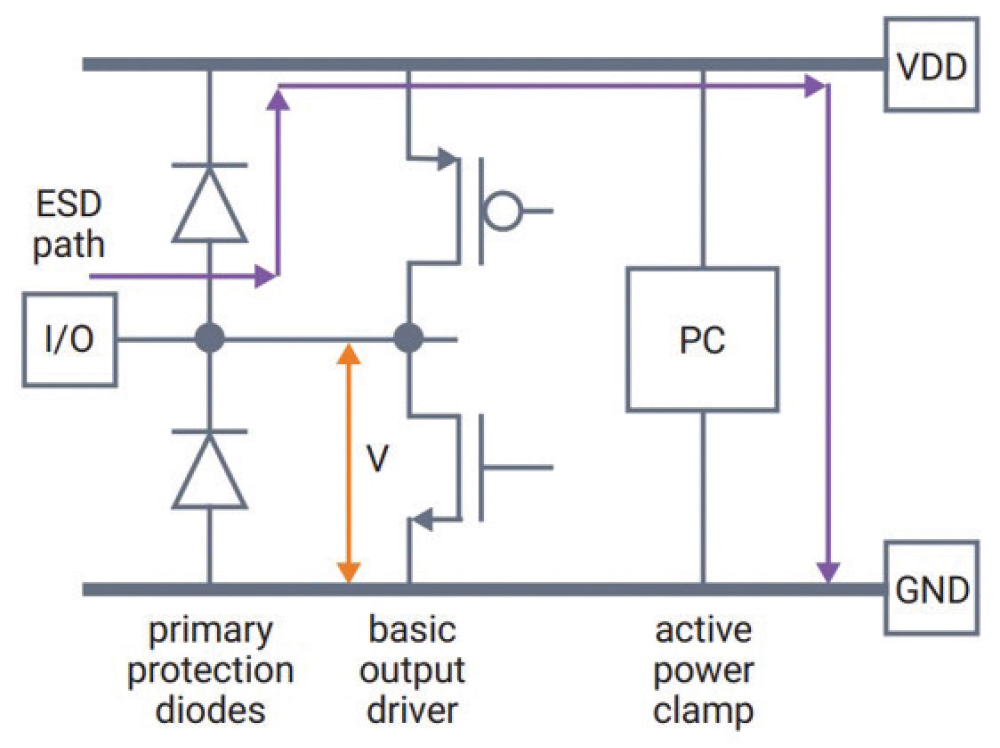
For many technology generations, this concept worked out well; transistor breakdown levels of junctions and gate oxide were sufficiently high compared to the clamping voltage. In the latest technologies, however, the breakdown voltages are reduced drastically to 4 V or less and the dual-diode concept clearly falls short in protecting the basic output driver configuration. In other words, the window of Figure 1 is rapidly closing.
The protection capability can be improved by increasing the diode and/or power clamp sizes. However, the gain will saturate and practically limit to ~1 V maximum, which is most likely not sufficient.
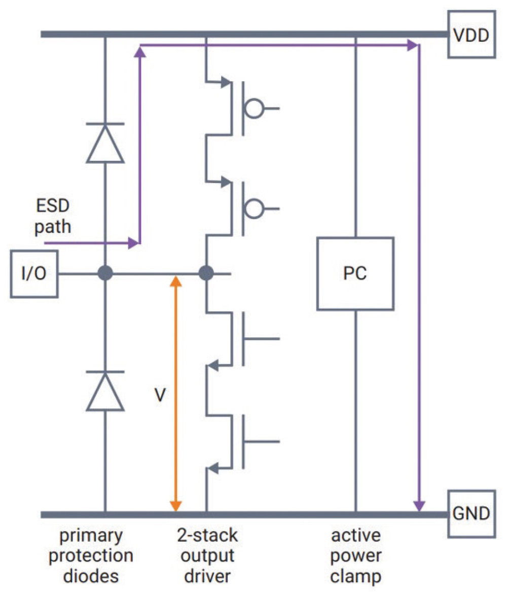
Another possibility to increase the ESD robustness is by using stacked driver transistors, as shown in the example depicted in Figure 3.
Compared to a single transistor driver, the junction breakdown voltage of the 2-stack transistor is higher, depending on the layout geometry of the transistor stack, up to a factor of two. The actual ESD network is unchanged, and so the resulting clamping voltage on the I/O pad is the same, but because of the higher breakdown voltage of the stack, the clamping level might just become sufficient to protect the 2-stack transistors. The concept is extendable to 3-stack, etc. to further increase the junction breakdown level. However, further stacking is no longer beneficial when the gate oxide breakdown becomes the critical constraint.
This concept has worked successfully in the past until the introduction of advanced planar technologies. In the latest FinFET technologies, however, the gain achieved by transistor stacking is generally not sufficient, and a fundamentally different approach is required to improve the robustness of the driver.
Essentially, a secondary ESD discharge path is achieved with extra diodes, separated from the primary dual diodes by a series resistor, dimensioned in such a way that the secondary circuit carries only a small fraction of the total discharge current. This small current, usually in the order of mA to tens of mA, causes a low voltage across the secondary diode, e.g., ~1.5 V. The voltage across the driver transistors, as shown in Figure 4, now determined by the voltage across the secondary diode and power clamp, reduces significantly (e.g., for the 6 A CDM example to ~3 V). The enhancement compared to the earlier estimated ~7.5 V at 6 A CDM in the case of primary protection only is significant.

To mitigate the problem of a large series resistor between the driver and pad, a suitable approach is to split the driver into parallel branches, each with its own (large) series resistor. Functionally, when the transistors are conducting, the resistors are in parallel, resulting in a low effective resistance during normal operation. From the ESD point of view, the high resistance in the individual branches counts (i.e., serves the intended purpose). The number of parallel branches should be chosen such that the targeted driver impedance is achieved.
To overcome the problem of the extra capacitance due to secondary protection diodes, an alternative approach of the secondary diodes is proposed in the next section.
The secondary current discharge path is achieved by the (forward-connected) parasitic diode of the driver transistors. These parasitic diodes can serve as a full replacement for explicit diodes when certain device and layout constraints are met. This advantageous approach saves the extra layout area needed for diodes and, more importantly, avoids performance loss due to explicit diode capacitance.


Another potential pitfall occurs when, for design-specific reasons, the transistor’s well (for example, the N-well of the PFET) is not connected to power. The parasitic diode exists but provides no (direct) discharge path to the power clamp. Thus, protection of the NFET is obstructed. A similar problem may occur for NFET in isolated P-well without a direct connection to ground. Depending on the applications, a possible solution is adding explicit protection diodes (stacked, if necessary) to power and ground.
- The effective diode size (drain diffusion area and perimeter);
- Anode-cathode spacing (drain diffusion to well contacts);
- Routing resistance from the well contacts to the nearest power clamp; and
- Current density requirement in the secondary current path.

Nevertheless, considering the low current through the secondary protections, the resistance realized by the diode implementation is by far not as critical as it is for the primary network. For instance, a resistance of 50 ohm gives a 10 mA current just 0.5 V extra voltage drop, which hardly reduces the huge advantage brought in by the secondary protection.
In summary, exact ESD characteristics of the parasitic diodes are preferred but not necessary. In practice, a set of guidelines regarding minimum diode size and maximum anode-cathode spacing, along with a routing resistance recommendation, are sufficient to make the parasitic diode approach successful.
Important topology checks on the driver schematic include:
- Any driver transistor should have a resistor with a minimum value (e.g., 200 Ω) between drain and I/O bump;
- All driver transistors should have dual diode (explicit and/or implicit) secondary protection;
- Secondary protection diode minimum dimension (area and/or perimeter) depending on the series resistor value; and
- Direct connection of the diodes to the power clamp.
- These topology checks on a schematic level ensure that a robust I/O architecture is applied.
- Supplementary checks on the layout level are also recommended to ensure the efficiency of the implementation. These include:
- Current density for all secondary protection components and connections;
- Anode-cathode spacing should not exceed the maximum distance (e.g., 1 µm), and
- Resistance of the diode connections to the power clamp should not exceed a maximum (e.g., 50 Ω).
The series resistor inherent to the secondary protection can be achieved by splitting the driver into multiple parallel paths. When secondary protection diodes can’t be implemented in high-speed SerDes designs due to the extra capacitive load, an alternative solution is to use the parasitic diodes of the driver transistors as secondary protection. Successful ESD co‑design also includes special care in the layout to ensure that the implicit protection is effective.
We strongly recommend the use of an appropriate EDA tool to check all I/O circuitry thoroughly for the presence of the secondary protections, either using explicit or implicit diodes, and to help ensure robust ESD designs. Besides topology on the schematic level, the checks should also include critical properties in the layout.
For the Synopsys high-speed SerDes IP portfolio, which includes PCIe 6.0, 112G, and 224G, optimal ESD withstand levels within the high-speed performance constraints are achieved by utilizing ESD co‑design. ICV PERC delivers an adequate verification solution for these IPs.
- ANSI/ESDA/JEDEC JS-001-2022, “Charged Device Model (CDM) – Device Level,” June 2021.
- ANSI/ESDA/JEDEC JS-001-2017, “Human Body Model (HBM) – Component Level,” May 2017.
- Industry Council on ESD Target Levels, “White Paper 2: A Case for Lowering Component Level CDM ESD Specifications and Requirements, Rev. 3.0,” May 2021.
- R. Ashton, “Updated Trends in Charge Device Model (CDM),” In Compliance Magazine, May 2023.