EMC concepts explained
Shielding to Prevent Radiation
Part 5: Near-Field Wave Impedance of Electric and Magnetic Dipoles
T

his is the fifth of seven articles devoted to the topic of shielding to prevent electromagnetic wave radiation. The first article [1] discussed the reflection and transmission of uniform plane waves at a normal boundary. The second article, [2], addressed the normal incidence of a uniform plane wave on a solid conducting shield with no apertures. The third article, [3], presented the exact solution for the shielding effectiveness of a solid conducting shield. The fourth article, [4], presented the approximate solution obtained from the exact solution. Both the exact and approximate solutions were derived for a good conductor in the far field of the radiating source. This article begins by discussing the topic of shielding effectiveness in the near field by introducing the concept of wave impedance.

Near-Field Shielding
Note: The following derivations are valid under the assumption that the shield made of a good conductor is much thicker than the skin depth, at the frequency of interest.

The total shielding effectiveness in the near field is:

equation
just like it was in the far field, but the reflection loss for electric sources is different from the reflection loss for magnetic sources (in the far field, the reflection loss for the two sources was the same).

The absorption loss in the near field is the same for the electric and magnetic sources and is the same as it was in the far field. That is:

equation
Thus, the shielding effectiveness in the near field for electric sources is:
equation
while the shielding effectiveness in the near field for magnetic sources is:
equation
Near-field shielding formulas for the reflection loss can be derived using the far-field shielding results for the reflection loss, and the concept of the near-field wave impedance for the electric and magnetic sources.
Hertzian (Electric) Dipole and Near-Field Wave Impedance
Hertzian dipole, shown in Figure 1, consists of a short, thin wire of length l, carrying a phasor current , positioned symmetrically at the origin of the coordinate system and oriented along the z axis.
Hertzian dipole
Figure 1: Hertzian dipole
The Hertzian dipole complete fields at a distance r from the origin can be obtained from the vector magnetic potential A shown in Figure 1 (see [5] for the derivations), and can be expressed as [6]:
equation
where:
equation
equation
where:
equation
equation
equation
where η0 is the intrinsic impedance of free space, and β0 is the phase constant. With this electromagnetic wave, we associate wave impedance, defined as:
equation
Using Equations (6) and (7) in Equation (8), we get [6]:
equation
At a small distance from the antenna, βr << 1, the term 1/(βr)2 will dominate the term 1/(βr), and the term 1/(βr)3 will dominate the term 1/(βr)2.

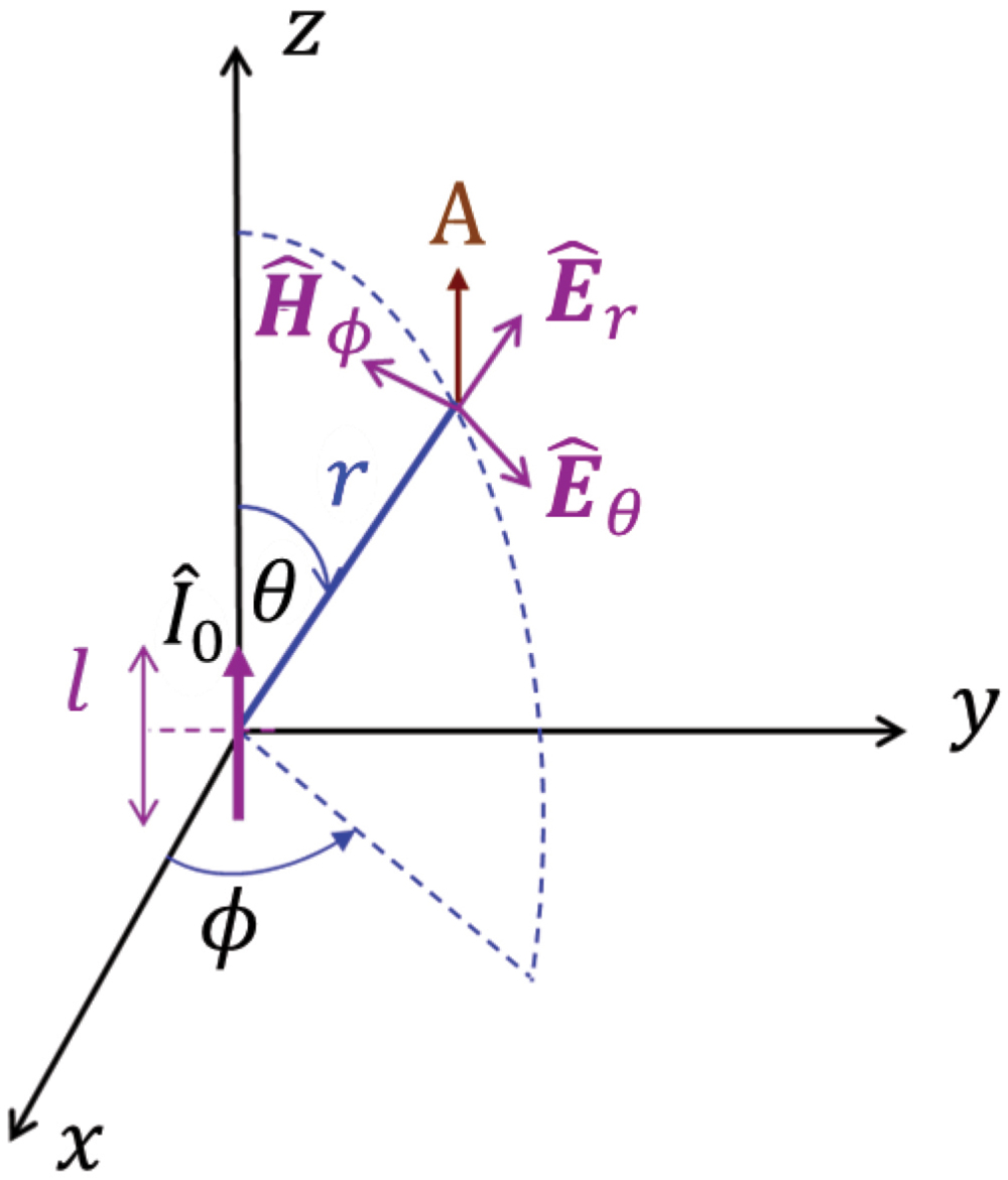
Thus, the wave impedance in Eq. (9) can be approximated by:

equation
or
equation
The magnitude of this wave impedance is:
equation
In the very near field:
equation
For that reason, we refer to the electric dipole as a high-impedance source. Since β0 = 2π / λ 0, we have:
equation
or
equation
In the next article, we will use this expression to evaluate the reflection loss RdB,e and the shielding effectiveness in the near field for electric sources, using Eq. (3), repeated here:
equation
Magnetic Dipole and Near-Field Wave Impedance
Magnetic dipole, shown in Figure 2, consists of a small thin circular wire loop of radius a, carrying a phasor current , positioned in the xy plane, with the center of the loop at z = 0.
Magnetic dipole
Figure 2: Magnetic dipole
The magnetic dipole complete fields at a distance r can be expressed as [6]:
equation
where:
equation
equation
where:
equation
equation
equation
The wave impedance for the magnetic dipole is defined as:
equation
Using Equations (17) and (19) in Equation (20) we get:
equation
At a small distance from the antenna, βr << 1, the term 1/(βr)2 will dominate the term 1/(βr), and the term 1/(βr)3 will dominate the term 1/(βr)2.

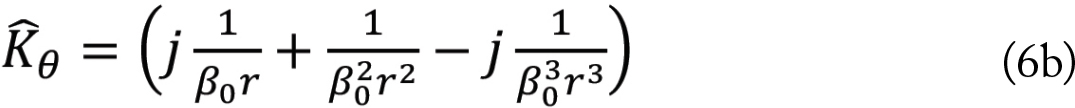
Thus, the wave impedance in Eq. (23) can be approximated by:

equation
or
equation
The magnitude of this wave impedance is:
equation
In the very near field:
equation
For that reason, we refer to the magnetic dipole as a low-impedance source. Since β0 = 2π / λ 0, we have:
equation
or
equation
In the next article, we will use this expression to evaluate the reflection loss Rdb,m and the shielding effectiveness in the near field for magnetic sources, using Eq. (4), repeated here:
equation
References
  1. Bogdan Adamczyk, “Shielding to Prevent Radiation – Part 1: Uniform Plane Wave Reflection and Transmission at a Normal Boundary,” In Compliance Magazine, June 2025.
  2. Bogdan Adamczyk, “Shielding to Prevent Radiation – Part 2: Uniform Plane Wave Normal Incidence on a Conducting Shield,” In Compliance Magazine, July 2025.
  3. Bogdan Adamczyk, “Shielding to Prevent Radiation – Part 3: Far-Field Shielding Effectiveness of a Solid Conducting Shield – Exact Solution,” In Compliance Magazine, August 2025.
  4. Bogdan Adamczyk, “Shielding to Prevent Radiation – Part 4: Far-Field Shielding Effectiveness of a Solid Conducting Shield – Approximate Solution,” In Compliance Magazine, September 2025.
  5. Bogdan Adamczyk, Foundations of Electromagnetic Compatibility with Practical Applications, Wiley, 2017.
  6. Clayton R. Paul, Introduction to Electromagnetic Compatibility, Wiley, 2006.
Share this story:
Bogdan Adamczyk headshot
Dr. Bogdan Adamczyk is professor and director of the EMC Center at Grand Valley State University (http://www.gvsu.edu/emccenter) where he performs EMC educational research and regularly teaches EM/EMC courses and EMC certificate courses for industry. He is an iNARTE-certified EMC Master Design Engineer. He is the author of two textbooks, “Foundations of Electromagnetic Compatibility with Practical Applications” (Wiley, 2017) and “Principles of Electromagnetic Compatibility: Laboratory Exercises and Lectures” (Wiley, 2024). He has been writing “EMC Concepts Explained” monthly since January 2017. He can be reached at adamczyb@gvsu.edu.