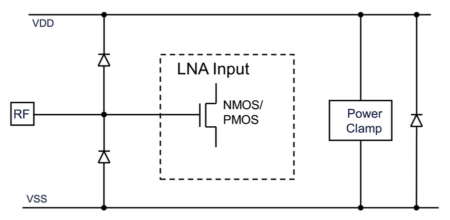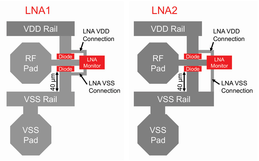
The device in this study is a Low Noise Amplifier (LNA) manufactured in a 28-nm technology. The input stage consists of thin-GOX MOS transistors with a breakdown voltage around 5 V. Due to RF performance requirements, the gate is tied directly to the pad, which is critical from an ESD point of view. The chosen ESD protection scheme is a standard rail-based topology as shown in Figure 1. To meet the capacitance requirement of <180 fF, small diodes were used as ESD clamping devices. The diodes have no Shallow Trench Isolation (STI) between the anode and cathode diffusions, and thus exhibit a fast turn-on time [1]. All protection devices, including a large dedicated power clamp, were placed in a close vicinity to the LNA (max 100 µm) to avoid any inductive paths and to minimize the bus resistance. The LNA is located directly below the input ball of the package. Since the receiving gates of the LNA are connected directly to the pad, a GOX damage can be detected by DC leakage testing.
CDM Head S-Parameter Simulation
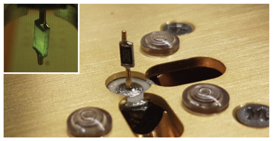
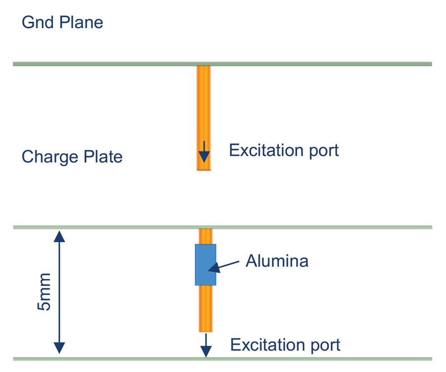
In [5] a method was demonstrated for measuring the S-parameters of a CDM head and simulating the resulting waveforms. In this work, we apply the same methodology but simulate the S-parameters with the 3D field solver HFSS from Ansys. Figure 7 shows the models used for simulation of the CDM head with and without resistor. The S-parameters are simulated at the excitation port between the pogo pin tip and the charge plate. The 1-MΩ resistor is simplified as a block of alumina interrupting the pogo pin.
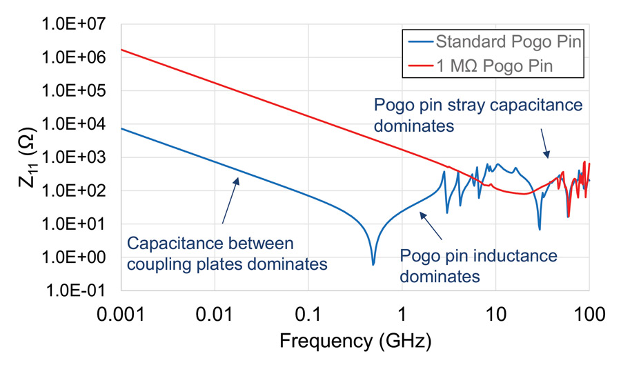
Figure 8 shows the simulated Z-parameters for the two configurations. Z-parameters are derived from the S- parameters and are easier to read since they represent the impedance seen into the pin tip. In the low frequency range the impedance decreases with increasing frequency as expected from a capacitance. For the standard CDM head the inductance of the pogo pin starts to dominate above 500 MHz and the impedance increases with the frequency. However, above 10 GHz the inductance loses its effect and the impedance remains in the order of 100 Ω up to 100 GHz. In this frequency range, the impedance with and without the resistor is similar. Thus, it is mainly the frequency spectrum of the discharge spark that determines the pulse shape in the upper frequency range, and it will be similar for the standard and the 1- MΩ pogo pin.
Rise Time of the CDM Spark
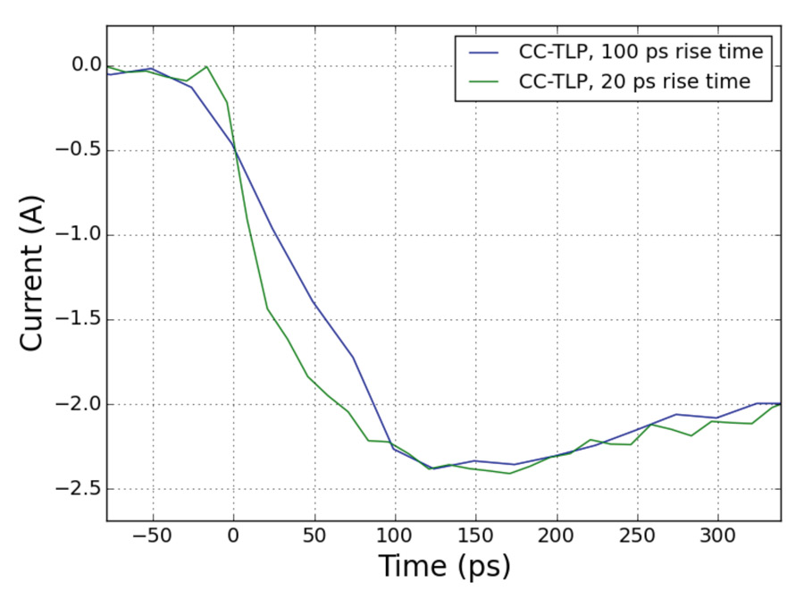
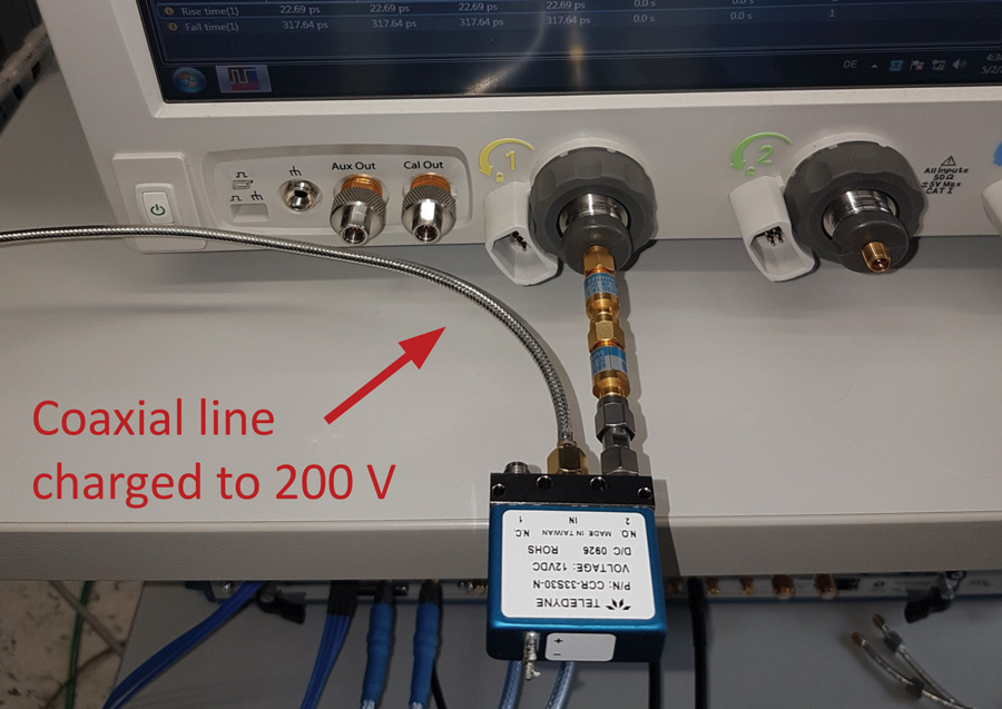
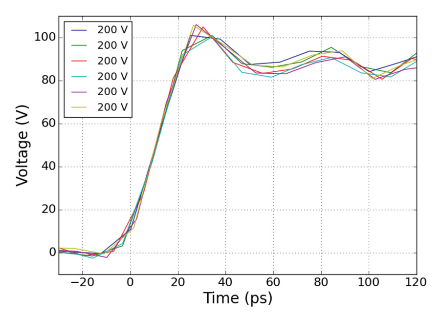
The most uncertain property of a CDM discharge event is the spark rise time and resistance. It varies strongly, depending on the applied voltage, air humidity, ball and pogo pin geometry and the speed of approach. In [6] it was shown that a CDM-like discharge between metal parts can have a rise time around 30 ps. To characterize an ideal metal-to-metal discharge a standard coaxial switch with 26 GHz bandwidth was used. The switch was connected in a TLP-like configuration with one port connected to a coaxial line that is charged up to 200 V. The other port of the switch was connected via attenuators directly to the input of an oscilloscope with 33 GHz bandwidth, shown in Figure 9. The coaxial switch is not an ideal TLP switch and shows strong pulse instability. Still, it was possible to capture several pulses with a rise time as low as 20 ps, as shown in Figure 10. Since the overall bandwidth of the setup is limited by the 18‑GHz rated connectors and attenuators, the rise time might be even faster. In this publication, a spark rise time of 20 ps was chosen for the simulations.
CDM Current Simulation Results
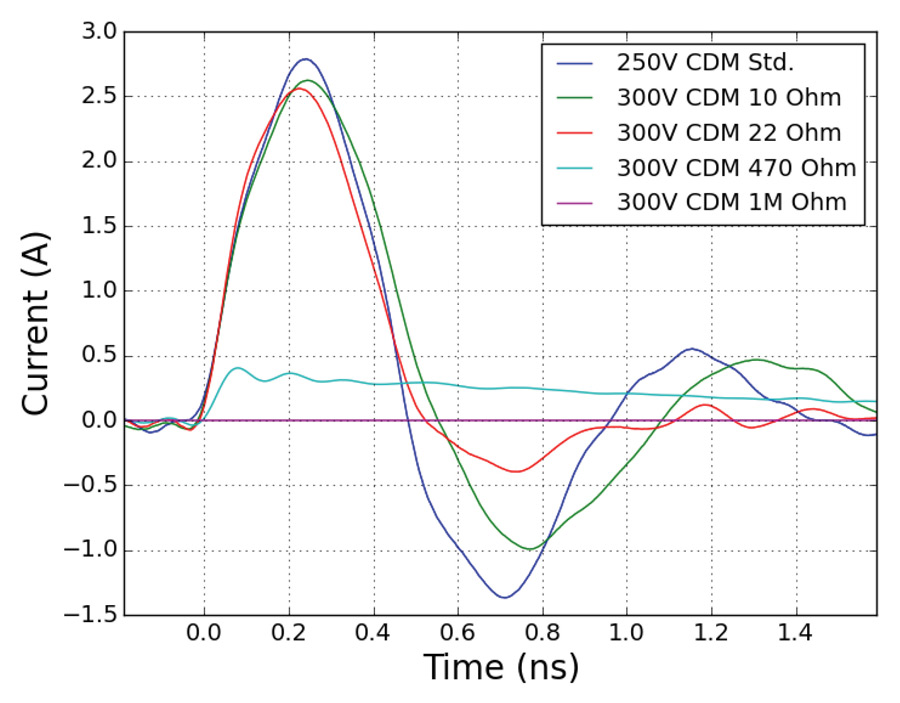
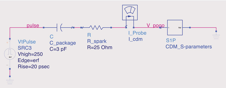
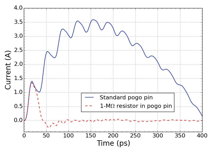
Simulation of the CDM current was performed in ADS from Keysight. The simulation schematic is presented in Figure 11. Since the simulated CDM head S-parameters don’t contain any package capacitance or spark resistance, the components C package and R spark have been added. C package was chosen to 3 pF to fit the CDM pulse shape, and R spark to 25 Ohm. The simulation results are presented in Figure 12 on page 24. The blue curve shows the discharge current from a standard CDM tester. Note that there is a first step in the waveform with about the 20-ps rise time of the pulse source. This corresponds to a current wave propagating along the pogo pin towards the ground plane, just like in a transmission line. When the wave reaches the ground plane, it gets reflected with a negative factor due to the low impedance of the ground plane. As a result, the amplitude is about doubled when the reflected wave reaches the pogo pin tip after about 50 ps. The current keeps increasing in steps until the peak amplitude is reached.
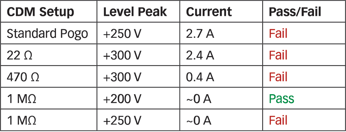
The first step also exists with the 1-MΩ resistor in the pogo pin, but the amplitude returns to zero after 40 ps since the resistor blocks the current flow. The comparison of both discharge waveforms and the fact that the damage occurs at the same CDM voltage level clearly demonstrates that the LNA is damaged by the current step at the onset of the CDM discharge.
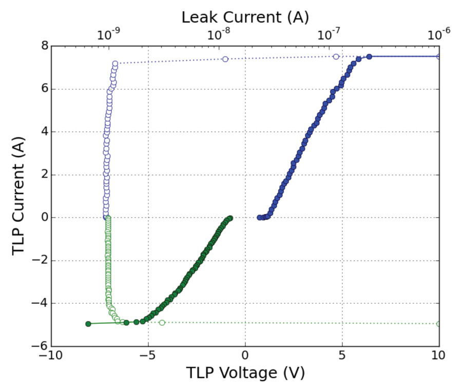
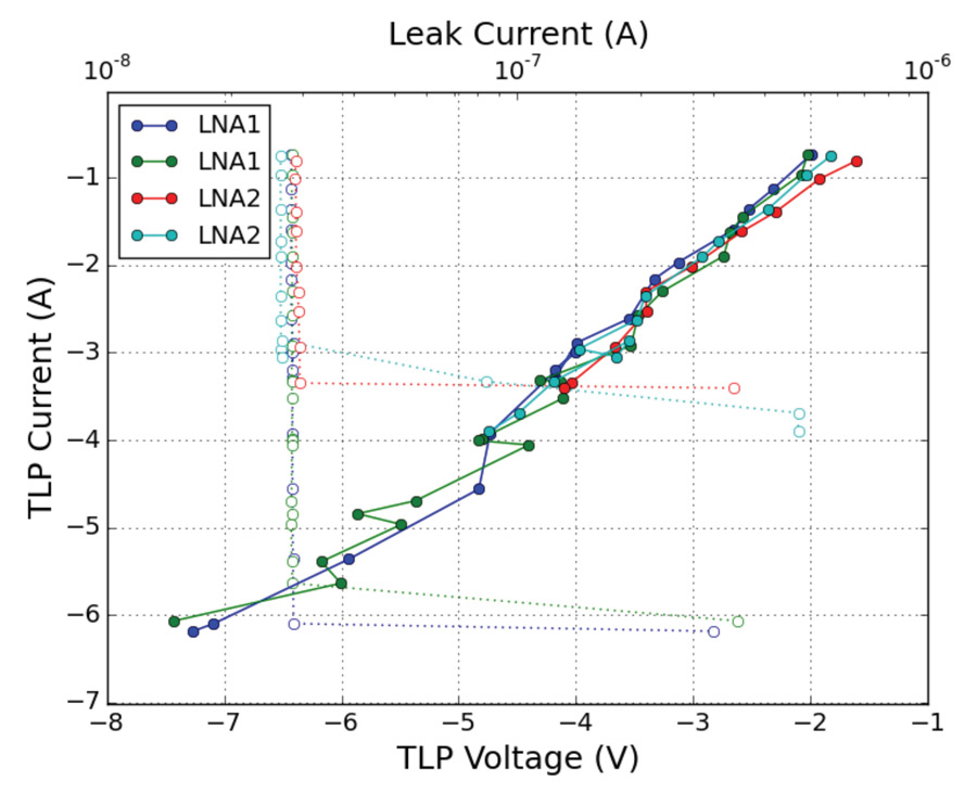
According to the simulation, the first step has an amplitude of about 1.4 A at 250 V charge level. This appears to be in the same range as where the LNA failed in CC-TLP testing with 20 ps rise time, considering that the CC-TLP probe was only capable of delivering a fast rise time up to 1.5 A according to Figure 3.
With such fast current slew rates, wire inductance and ESD device turn-on time play an increasing role. Even short traces with an inductance in the order of 10 pH will create a voltage drop of several volts. For RF optimized designs with a short low-loss path from the ball to the sensitive gate, this poses a serious threat that needs to be addressed in the ESD design.
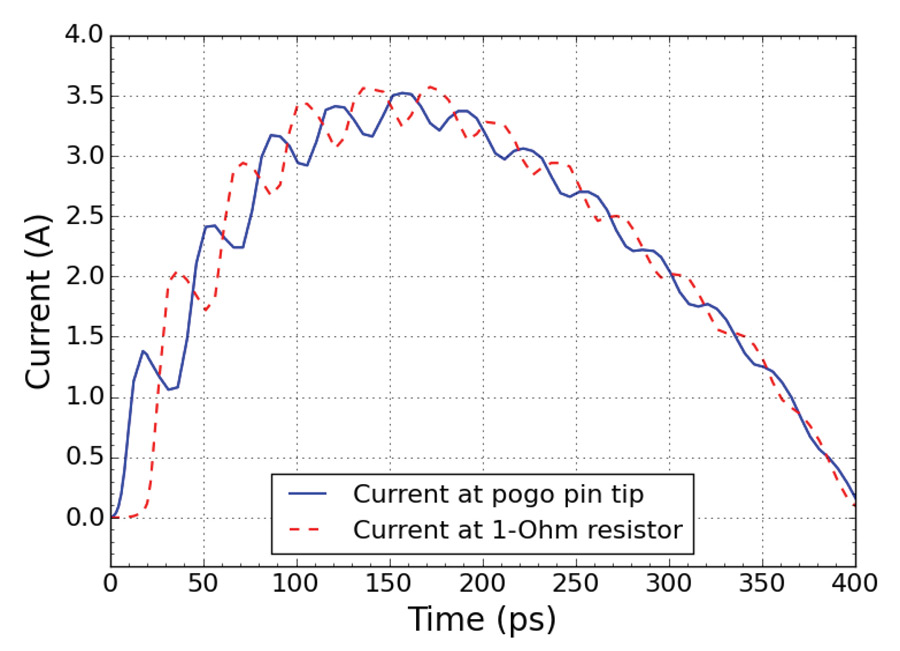
CDM probe heads with a bandwidth of 20 GHz have been reported [7], but can a CDM probe head really measure the current at the pogo pin tip? This is investigated by performing a simulation with an additional excitation port between the pogo pin and the ground plane. The CDM waveform is simulated with an ideal 1-ohm resistor to ground at the second port according to Figure 13. Hence, the current flowing through the 1-ohm resistor to the ground plane can be obtained, which is the current an ideal CDM probe would capture. The simulation result is presented in Figure 14. It is seen that an equally fast rising pulse arrives at the 1-Ω resistor with a time delay of about 20 ps. However, the current of the first step has a higher amplitude than the current entering the tip. This can be explained by the impedance mismatch that appears when terminating the pogo pin into a 1- ohm load. Theoretically, the current would double when terminating into close to a short circuit, but since the pogo pin is not a perfect transmission line, there will be losses.
It has been shown that a CDM probe head can principally measure the fast initial step, but the waveform will not be identical to the current entering the pogo pin.
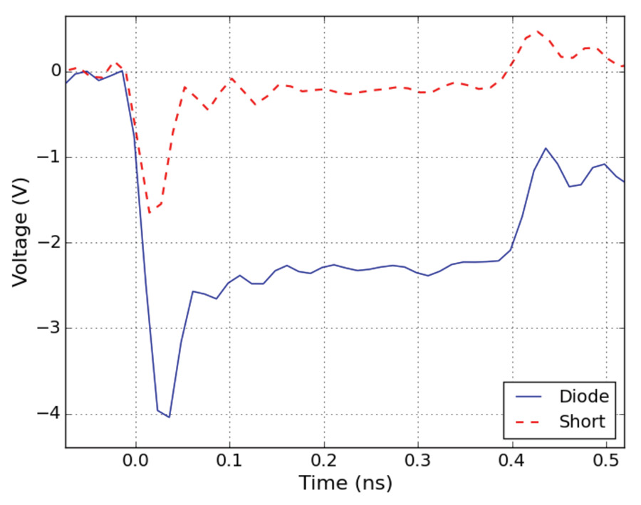
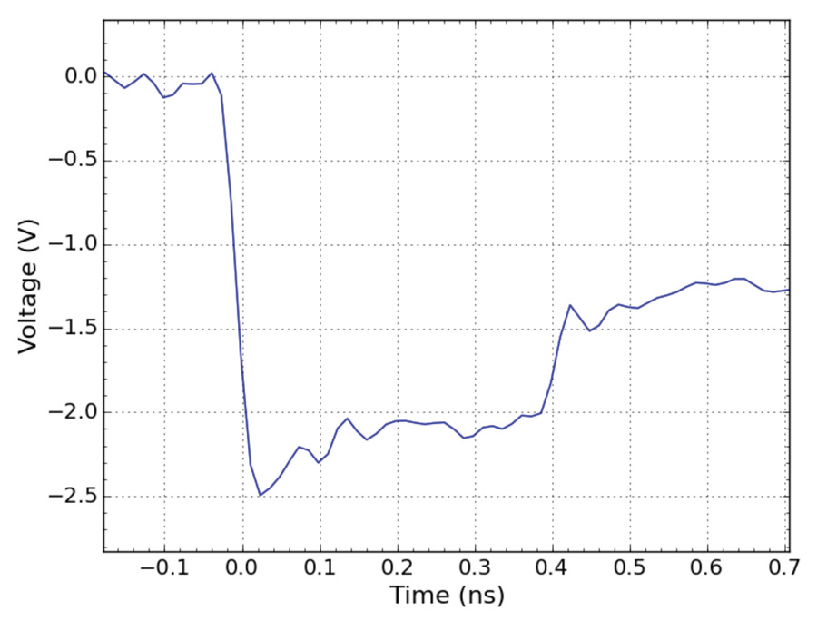
To assess the performance of the ESD protection a diode test structure on wafer was measured with the fast TLP source presented in section IV.B.2. The diode size was about twice as large as used in the ESD protection for the LNA. RF probes of type Cascade Infinity with a bandwidth of 40 GHz were used in TDT configuration. With a fast rise time of 20 ps the wiring inductance will cause a considerable inductive voltage drop. In order to eliminate this contribution, a de-embedding structure with the same metallization, but short-circuited in the lowest metal layer, was also measured. Hence, it is possible to assess the voltage contribution from the diode alone by subtracting the de-embedding waveform. In Figure 15 the voltage response of both the diode and the de-embedding structure at a current of -3 A are plotted. The voltage response after subtraction of the de-embedding waveform is presented in Figure 16 on page 26.
The diode shows 2 V clamping voltage with an overshoot of 0.5 V. This should be considered a very fast diode with a turn on time of less than 50 ps. This can typically not be achieved with STI-bound diodes or SCR based devices.
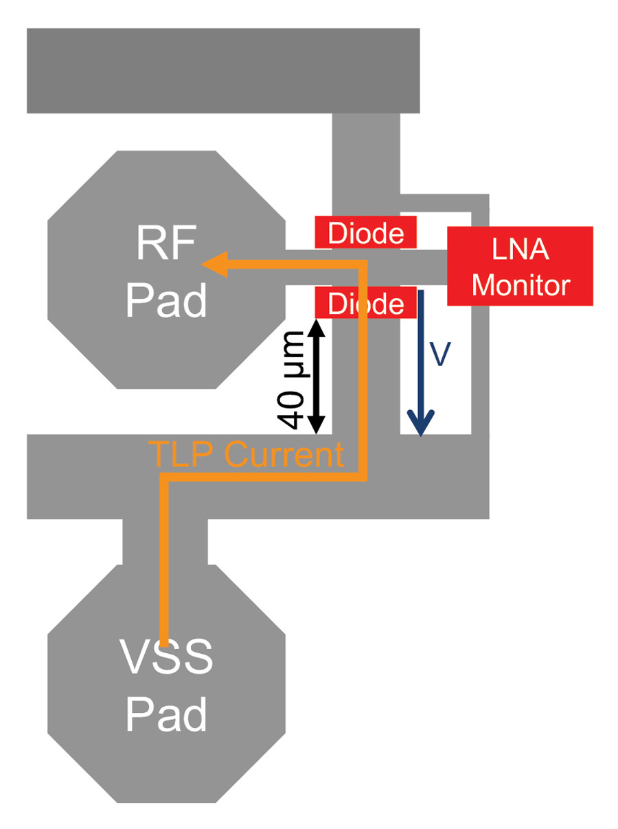
The lower failure level of -3 A for LNA2 can be explained by the additional voltage drop appearing across the vertical connection down to the VSS rail. In Figure 19 the current path from the VSS pad to the RF pad has been drawn for LNA2. It is evident that the voltage drop across the vertical VSS trace between the diode and the VSS rail will be visible at the LNA monitor. It can be estimated that the 40-µm long trace will have about 40 pH of inductance. The resistance in the path is in the order of milliohms and can be neglected.
With a current slew rate of 3 A in 20 ps the voltage drop can be expressed as:
V = dI/dt * L = 3 A / 20 ps * 40 pH = 6 V
It seems plausible that an additional voltage drop of 6 V is enough to damage the gate oxide of the LNA monitor even for the very short stress time of 20 ps.
A similar VSS routing weakness could be identified in the LNA product. After redesign with improved routing, the product was able to meet the CDM requirements.
It has been shown that the fast initial step of the CDM pulse damages the sensitive GOX of the investigated LNA. The exact rise time is not accessible, but it could be proven to be 20 ps or less. All test methodologies using 100 ps rise time failed to reproduce the CDM failure by a factor of two. This applies to VF-TLP and CC-TLP, but would also be the case for alternative CDM testing methods such as Contact CDM (C-CDM) or CDM2.
The failure mode from CDM testing could be reproduced by applying CC-TLP stress with a rise time of 20 ps. However, it is not straight forward to correlate the CC-TLP current slew rate with a certain CDM stress level. For the investigated LNA the CC- TLP fail level for positive and negative polarity only differed by 25% (+3 A / -2.4 A). However, in CDM testing the difference was as high as 60% (+250 V / ‑400V). This discrepancy is not yet understood, but it is believed that the polarity might have an impact on the spark rise time. These phenomena need to be fully understood before alternative CDM stress methods can be applied for qualification.
Since the exact voltage level in a CDM tester varies in a wide range depending on the calibration, the level of the first step will depend on the calibration as well. This introduces an additional source of error.
As perspective to real-world relevance, it should be mentioned that the first current step should not be considered as a tester artifact. The phenomenon takes place whenever a charged device is approached and touched by any metal object.
An improved high bandwidth TLP characterization method is needed to accurately assess the ESD design of sensitive RF interfaces.
- M.-D. Ker, K.-K. Hung, H.T.-H. Tang, S.-C. Huang, S.-S. Chen, M.-C. Wang “Novel diode
- Structures and ESD Protection Circuits in a 1.8 V 0.15 µm Partially-Depleted SOI Salicided CMOS Process”, Proceedings of 8th IPFA, 2001, pp. 91-96.
- H. Wolf, H. Gieser, W. Stadler, W. Wilkening, “Capacitively Coupled Transmission Line Pulsing CC-TLP – A traceable and reproducible Stress Method in the CDM Domain”, EOS/ESD 2003.
- J. Weber, K. T. Kaschani, H. Gieser, H. Wolf, L. Maurer, N. Famulok, R. Moser, K. Rajagopal, M. Sellmayer, A. Sharma, H. Tamm, “Correlation study of different CDM testers and CC-TLP”, EOS/ESD 2017.
- J. Barth, J. Richner, “Improving CDM Measurements With Frequency Domain Specifications”, EOS/ESD 2016.
- F. z. Nieden, K. Esmark, S. Seidl, R. Gärtner, “Predict the Product Specific CDM Stress Using Measurement-based Models of CDM Discharge Heads”, EOS/ESD 2016.
- P. Tamminen, R. Fung, R. Wong, “Charged device ESD threats with high speed RF interfaces”, EOS/ESD 2017.
- D. Helmut, H. Gieser and H. Wolf, “Simulation and Characterization of Setups for Charged Device Model and Capacitive Coupled Transmission Line Pulsing”, ESD-Forum 2015.
