hot topics in ESD
Even Optical Communication Needs ESD Protection
I

n the past, fiber-optic communication was used primarily for long-distance communication (50 km and beyond). Only a limited number of these high-end interface products were required worldwide. More recently, companies running large data centers (Facebook, Google, Amazon) have been replacing the traditional copper cabling between server racks (Figure 1). The copper-based approach is considered a bottleneck for further improvements in data transfer capacity. Optical communication can dramatically increase the bandwidth between servers while reducing complexity, power consumption, and cost.
Reducing Cost and Power while Increasing Bandwidth
Thus, the optical interconnect suppliers now need to produce a large number of their products. To reduce the cost, they separate the optical parts (laser diodes, photodetectors) from the digital controller circuits. For the electrical ICs, regular CMOS technology can be used for mass-production. Moreover, there were several technological breakthroughs in the last decade, where conventional CMOS processing steps facilitate the creation of several different optical components like WDM (Wavelength Division Multiplexers), lasers, detectors, waveguides in, e.g., SOI processes.
Hybrid 2.5D and 3D Integration
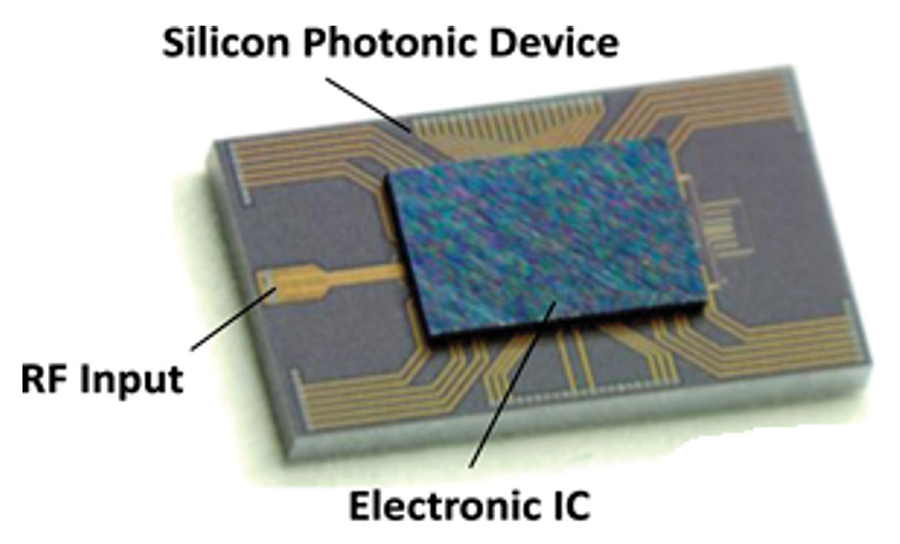
Both optical and electrical elements are then combined within a single IC package using advanced packaging techniques like 2.5D (electronic interposer – Figure 2 on page 14) and 3D (flip-chip – Figure 3 on page 14) integration. The hybrid integration allows designers to select the best process option for each function; for example, the digital functions can be integrated in high‑end CMOS technology with high performance and smaller size. The photonic die does not benefit from this minimum feature size and can thus be designed in a more mature SOI technology, which significantly reduces the total cost.
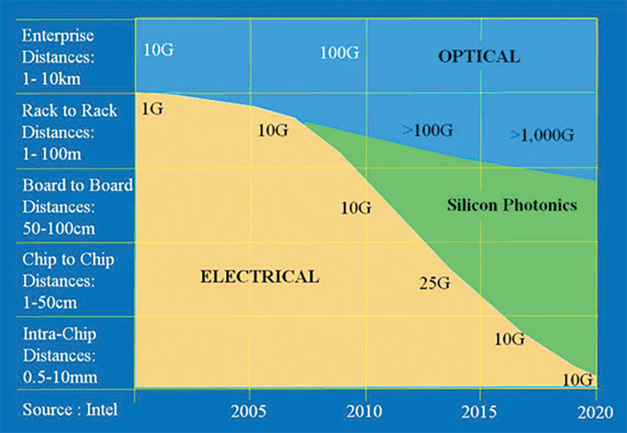
Figure 1: The engineers from the Intel groups working on optical communication summarized the potential for Silicon Photonics for different interface distances
Figure 1: The engineers from the Intel groups working on optical communication summarized the potential for Silicon Photonics for different interface distances [1]. The traditional optical communication will be used mainly for the long distances. Silicon photonics will replace the electrical communication for the shorter distances thanks to the combination of low power, low cost, and high bandwidth opportunity.
Optical Links Need Custom ESD Clamps
The electronic IC that is used to control the optical parts and to process the signals before transmitting or after receiving is manufactured using advanced CMOS technology like 28nm or below. The interfaces consist of high speed (25Gbps or higher) SerDes-type circuits.

To create such high-speed differential circuits, designers utilize the thin oxide transistors. However, those transistors are very sensitive and can be easily damaged during transient events like electrostatic discharge (ESD). The maximum voltage that these transistors can endure during transient events is 4V or less.

Even though the sensitive pads are not connected outside of the package, they could still receive ESD stress during assembly. Therefore, adequate protection clamps need to be inserted at the bond pads. On the other hand, for signal integrity, it is important to limit the capacitance between the interface pads and the supply lines. Selecting on-chip ESD protection with low parasitic capacitance has been studied by several authors in the past. Diode or SCR based protection concepts have been used for RF chips [4-8]. However, for the most sensitive interfaces running at low voltage, ESD protection based on dual diode at the I/O, combined with a (distributed) power clamp, is not always feasible [8].

Figure 2: 2.5D integration of optical and electrical IC (CPU) [2]
Figure 3: Packaging of an electronic IC (driver) on a silicon photonic device using a flip-chip bonding process
Fortunately, the ESD rating for these interfaces can be reduced. Because this flip-chip assembly is performed in an ESD controlled environment, the ESD protection level could be reduced to 200V HBM or sometimes even 100V HBM without effect on the yield. Because the high-speed interfaces are not exposed outside of the product/package assembly, they need to be considered as inter-domain interfaces.

Many advanced CMOS foundries provide a set of I/O and ESD protection circuits that designers can use. However, these standard, general-purpose, interface blocks are not suitable for the Silicon Photonic designs for the following reasons:

  • The leakage from the general-purpose ESD blocks is too high
  • The high-speed interfaces typically operate at a voltage level below the standard I/O voltage levels (1.0V or lower compared to 1.8V, 2.5V or 3.3V for the IO circuits)
  • The high-speed SerDes circuits cannot tolerate a lot of parasitic capacitance or resistance added to the signal path. A typical analog I/O introduces 150fF of parasitic capacitance, well above what can be tolerated by the circuit.

Companies developing optical communication products are looking for improved solutions for the protection of the high-speed interfaces (Tx, Rx), and the low voltage power pads on the electronic die. Two case studies are included below.
Example 1: ESD Protection for 28Gbps Interface in 28nm CMOS
For the regular, low speed I/Os at 1.8V, the Analog/digital I/O library provided by the foundry was sufficient. The ESD requirement for those pads was 2kV HBM. On the other hand, the analog I/Os in the foundry library introduced too much parasitic capacitance for the high-speed interfaces. The designers requested a reduced total capacitance of the ESD device below 15fF.
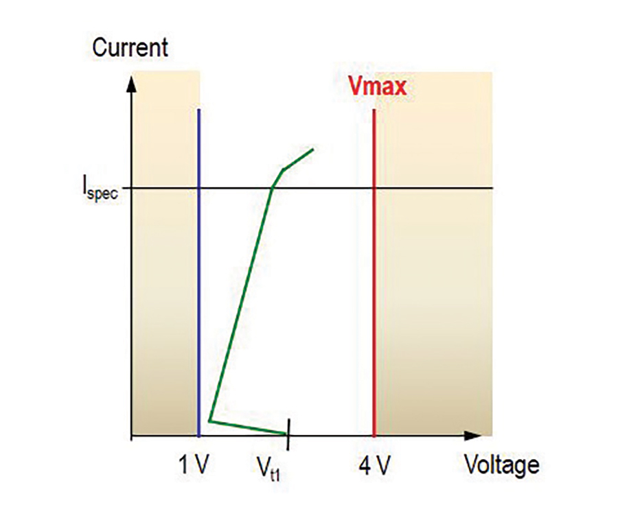
Figure 4: ESD design window for the 28Gbps interface in 28nm CMOS.
Figure 4: ESD design window for the 28Gbps interface in 28nm CMOS. The ESD protection trigger voltage must be below 4V, and failure current must be above 130mA (200V HBM)
The 28nm CMOS SoC was co-packaged with a silicon photonic device in a shared/hybrid integrated package. The assembly is performed in an ESD controlled environment. The ESD protection level was reduced to 200V HBM [9], roughly 130mA during 100ns TLP stress.

The 28Gbps interfaces used a differential pair concept. The 1V functional circuit is created using 0.9V core transistors to ensure the switching speed can be reached. However, these transistors are very sensitive during ESD stress. The available ESD design window (Figure 4) for the Rx, Tx signals is reduced to 4V. Other requirements for the ESD protection included low leakage operation and small silicon footprint (right side of Figure 5). The leakage at 1V bias is below 50pA at room temperature and less than 50nA at 125°C.

The ESD protection design consists of a full local protection clamp concept (Figure 5 on page 15). A 1V power clamp was integrated to ensure all the stress cases could be handled locally at the interface, and bus resistance is taken out of the equation. The entire clamp structure was isolated from the substrate to reduce noise from the substrate that could come from digital circuits further on the die.

The total parasitic capacitance at the I/O pad consists of different aspects. The junction capacitance can be easily derived from the foundry provided Spice models for diodes. The metal connections to the local ESD clamps can add a significant amount of capacitance. The parasitic metal capacitance can be derived from PEX (parasitic extraction) calculations. Reducing the width of the metal connections can reduce the capacitance but will also reduce the robustness of the connection. The minimal metal width is derived from ESD stress performed at different metal stripes on our ESD test chip. Metal dummies (a requirement for CMP in advanced processes) are included in the PEX extraction when customers request ESD protection with ultra-low capacitance (well below 100fF).
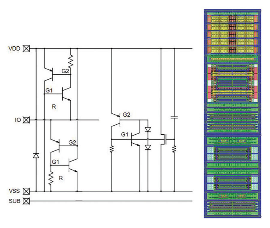
Figure 5: Schematic view (left) of the full local protection approach for the Rx and Tx nodes of the SerDes circuit.
Figure 5: Schematic view (left) of the full local protection approach for the Rx and Tx nodes of the SerDes circuit. It is based on Sofics proprietary ESD-on-SCR devices. An SCR based 1V power clamp is integrated into the same layout (right). The total area for ESD is 683.75 um2.
Through an iterative process (layout, PEX extraction), the total parasitic capacitance of the ESD clamp was reduced to less than 15fF. The plot shown in Figure 6 illustrates the capacitance value as a function of the bias voltage at the pad.

In the iterative process to reduce the contribution of the parasitic capacitance from the metal connections, a number of rules are used:

  • Remove unnecessary via connections
  • Reduce Metal 1 as much as possible, keep it on top of the connected diffusion only.
  • Prevent running Metal 1 across junctions.
  • Vertical connection to higher-level metal layers to reduce capacitance from intermediate metal levels

Even when reduced, more than 40% of parasitic ESD capacitance can be linked to the metal connections in advanced nodes.
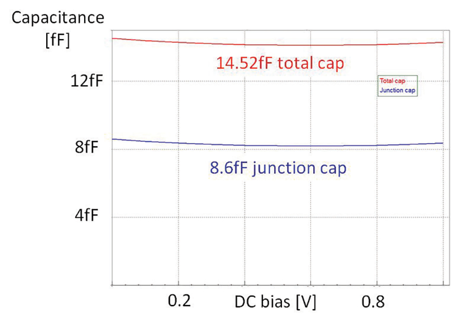
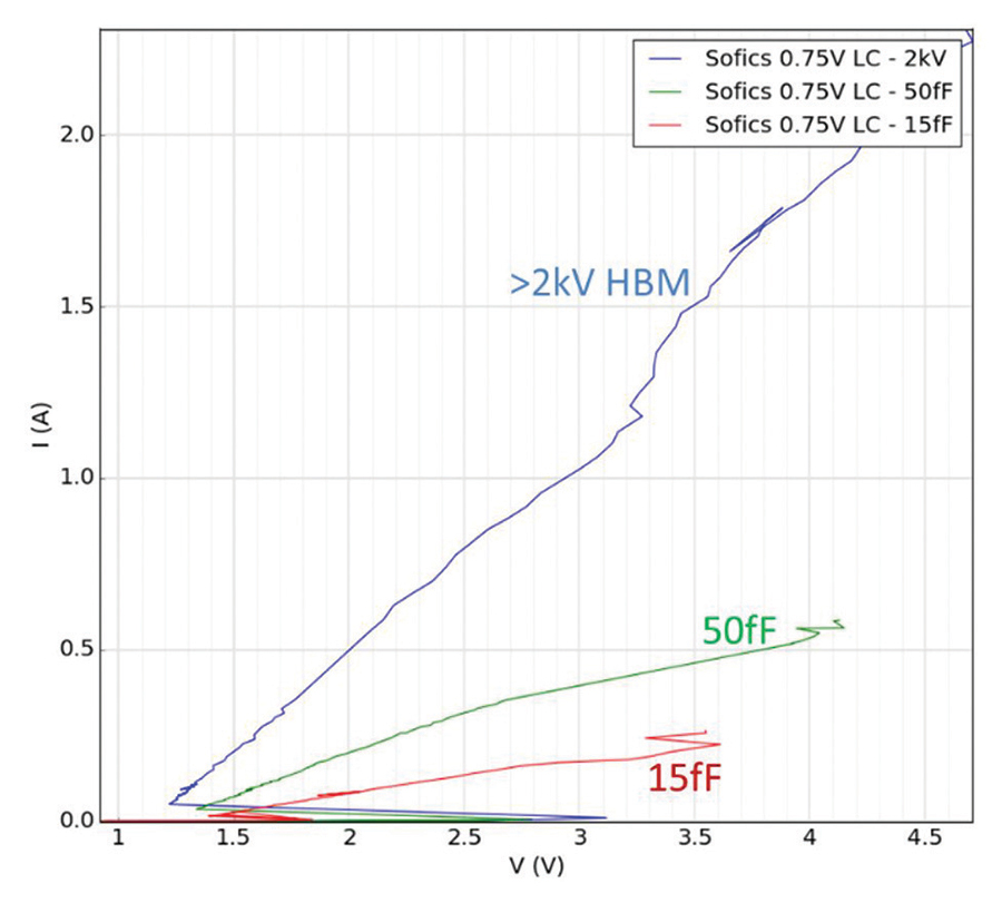
Figure 6: Parasitic capacitance (total and junction only) across the I/O voltage for the full local ESD protection clamp designed in a TSMC 28nm technology
Figure 7: Silicon results on the TSMC N7 process. TLP results for three versions (with different target requirements) of the ESD concept.
Example 2: Silicon Photonics Solution on N7 FinFET
To further increase the bandwidth of the optical interconnects (beyond 56 Gbps), our customer moved to TSMC 7nm FinFET technology. The proposed ESD solution is similar to the previous case (Figure 5). Two versions of the ESD protection are created, one with parasitic capacitance of 50fF, and a smaller version with less than 15fF. Measurements on TSMCs 7nm FinFET process demonstrate that the SCR based local clamp performs as expected (Figure 7).

In 7nm technology, the failure voltage of core transistors (gate to source and drain to source) is about 3V. Fortunately, in many SerDes applications, there is a bit more margin due to other transistors connected in series. Failure voltage under ESD conditions of those circuits is around 4-5V depending on the circuit concept – similar to the design window shown in Figure 4.
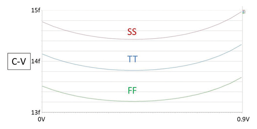
Figure 8: Simulation of the parasitic capacitance of the 15fF version on 7nm, across applied IO voltage, and for three corners.
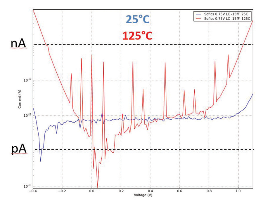
Figure 9: Leakage measurement at low (25°C) temperature and high (125°C) temperature.
Figure 9: Leakage measurement at low (25°C) temperature and high (125°C) temperature. Even at high temperatures, the leakage of the ESD solution remains below 1 nA within the entire voltage range (0 to 0.75V).
The 7nm low-capacitance ESD clamps have been integrated into two designs for high-speed interfaces. The simulated parasitic capacitance over IO voltage for the 15fF version is shown below (Figure 8) for the Typical, Fast and Slow corners. It includes both the junction capacitance (from the Spice model) and Metallization capacitance (based on PEX extraction). The SerDes circuits typically operate below 1V.

Besides low parasitic capacitance, the SCR based solution also has a low leakage, orders of magnitude lower compared to the ESD solution proposed by the foundry. The leakage measurement for the 15fF version is shown in Figure 9.

Conclusion
Silicon photonics can enable a strong growth of the (optical) communication market. Thanks to the mass production opportunity of both the optical and electrical dies and the availability of 2.5D and 3D hybrid integration all the requirements can be met: lower power, lower cost, high volume, high bandwidth.

High-speed SerDes interfaces integrated with Silicon photonics products need adequate protection with minimal parasitic capacitance. In this article, we demonstrated ESD protection clamps for 28 to 56Gbps interfaces in TSMC 28nm and TSMC N7 FinFET. Record-low parasitic capacitance levels below 20fF were achieved while ESD robustness is guaranteed.

References
  1. Lisa Huff, “Silicon Photonics – Are We Past the Hype?” http://www.connectorsupplier.com, 2015
  2. Fujitsu press release, http://www.fujitsu.com/global/about/resources/news/press-releases/2011/0916-01.html, 2011
  3. D. Thomson, et al., “Roadmap on Silicon Photonics,” Journal of Optics, volume 18, # 7, 2016.
  4. M.K. Radhakrishnan, et al., “ESD Reliability Issues in RF CMOS Circuits,” 2001.
  5. Feng K., et al., “A comparison study of ESD protection for RFICs: performance versus parasitic,” IEEE RFI, 2000.
  6. RMD.A Velghe et al., “Diode Network Used as ESD Protection in RF Applications,” EOS/ESD Symposium, 2001.
  7. K. Bhatia et al., “Layout Guidelines for Optimized ESD Protection Diodes,” EOS/ESD Symposium, 2007.
  8. G. Boselli, et al., “Analysis of ESD Protection Components in 65nm CMOS: Scaling Perspective and Impact on ESD Design Window,” EOS/ESD Symposium, 2005.
  9. J. Van der Borght et al., “Protecting Photonics Where Diodes Fail: ESD Protection for 28 to 56 Gbps Interfaces in 28nm CMOS,” International ESD Workshop 2018, Belgium.
Share this story:
Bart Keppens headshot
Bart Keppens received an engineering degree in electronics from Groep T, Leuven in 1996. Bart has co-authored more than 40 peer-reviewed published articles. He has been a member of the Technical Program Committee for the EOS/ESD Symposium since 2003. Bart holds several on-chip ESD protection design patents.
ESD Association black logo
Founded in 1982, EOS/ESD Association, Inc. is a not for profit, professional organization, dedicated to education and furthering the technology Electrostatic Discharge (ESD) control and prevention. EOS/ESD Association, Inc. sponsors educational programs, develops ESD control and measurement standards, holds international technical symposiums, workshops, tutorials, and foster the exchange of technical information among its members and others.