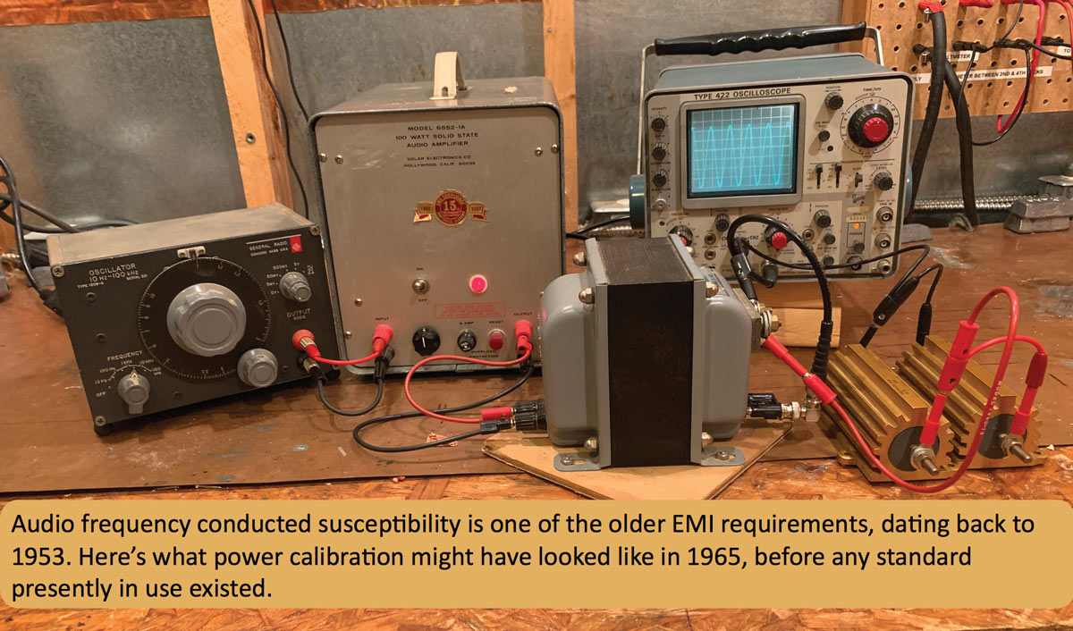
his technical tip presents safer ways of performing audio frequency conducted susceptibility testing than the standard approach described in References 1-8. “Safer” here means reducing the probability of accidentally damaging the test article, either by over-testing, or by inducing instability in the test article’s internal switched mode power supply, or by causing a shutdown of the audio amplifier resulting in possible instability in the test article internal switched mode power supply.
These are always important considerations, but especially so when the test article is a one-of-a-kind item whose delivery is on the program schedule critical path. Finally, the stability issue is most pronounced when the test article runs off a dc bus, because dc/dc converters tend to have much smaller hold-up capacitors out front than if the cap providing the hold-up function also has to smooth out ripple from a 50/60/400 Hz ac bus.
A prime example of a sensitive load running off a dc bus is equipment used on spacecraft and launch vehicles. Further, such may be one-of-a-kind items where the actual flight unit is being EMI qualified.
References 1-8 provide similar limits and test methods. Spacecraft audio conducted susceptibility limits and test methods are based on various issues of MIL-STD-461/-462, References 1-5 (viz. AIAA S-121, Reference 9). As found in Reference 9, most spacecraft audio conducted susceptibility limits are tailored much lower than the limits found in any of References 3-5, for reasons described in Reference 10.
Another difference between References 1-5 and spacecraft derivatives is that the spacecraft derivatives tend to compute a power limit based on the dc voltage limit, whereas MIL-STD-461 CS01/CS101 use the power from the higher ripple limit for higher potential (ac) buses. This results in the use of amplifiers of at least 100 W output, and often 300 W or higher. Further, many such amplifiers have quite low output impedances, so that they can deliver much more than the pre-calibrated power if the input impedance of the test article dips below 0.5 Ω. To promote safety, it is advisable to use no more power than is absolutely necessary and to have an output impedance of around 2 Ω (which transforms to 0.5 Ω across the coupling transformer windings).
An added benefit to a series output resistor on a low output impedance amplifier is protecting that amplifier from reflected ac ripple when the test article is powered from an ac (50/60/400 cycle) power bus. If the added resistor is large with respect to the actual amplifier output impedance, most of the reflected ac ripple drops across the added resistor, not the amplifier output itself.
In this tech tip, two approaches to protecting against such problems are explored. One uses a low rather than high-power amplifier, and the other technique inserts an attenuator between the output of a high-power amplifier and the coupling transformer primary. The attenuator prevents too much power in the event of an operator error, but also places an effective 2 Ω resistance across the primary of the transformer even if the amplifier goes open so that the test article will never see more than 0.5 Ω inserted between itself and the power source on account of the coupling transformer.
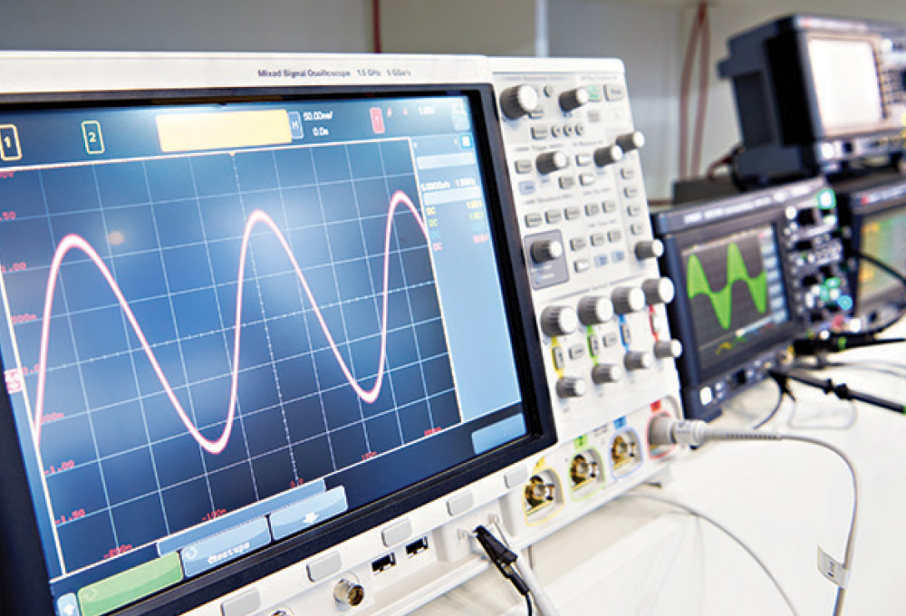
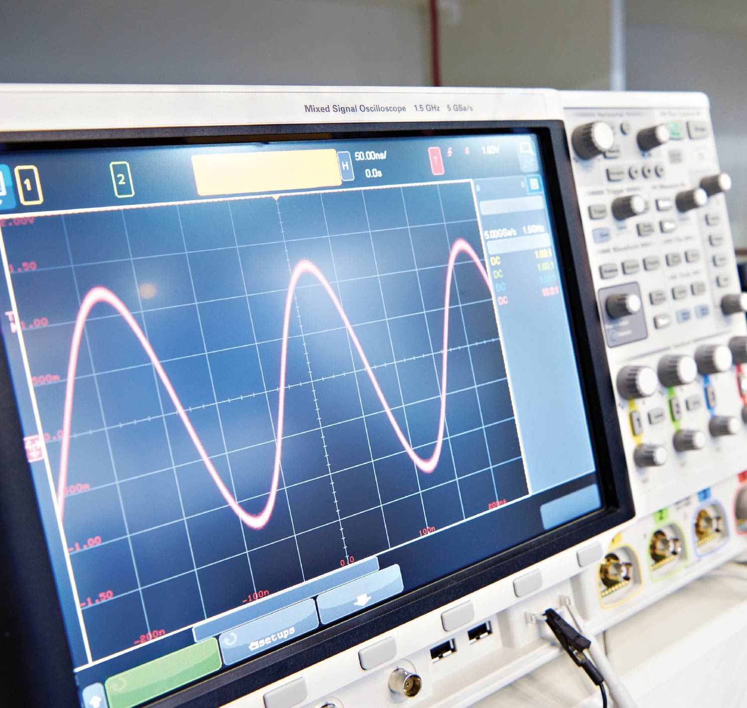
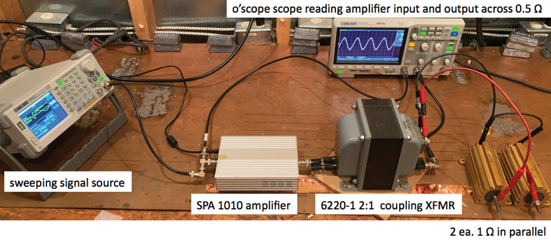
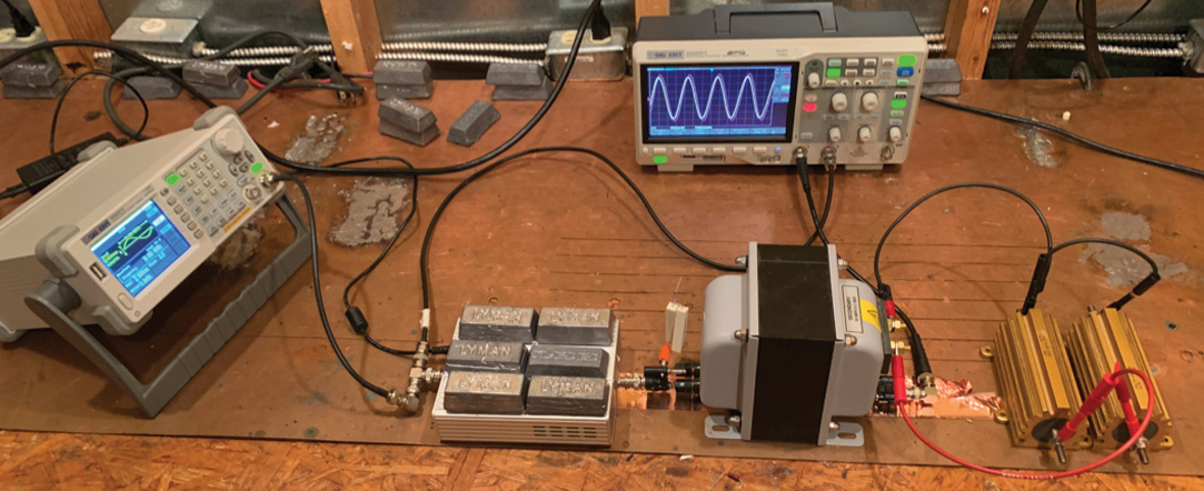
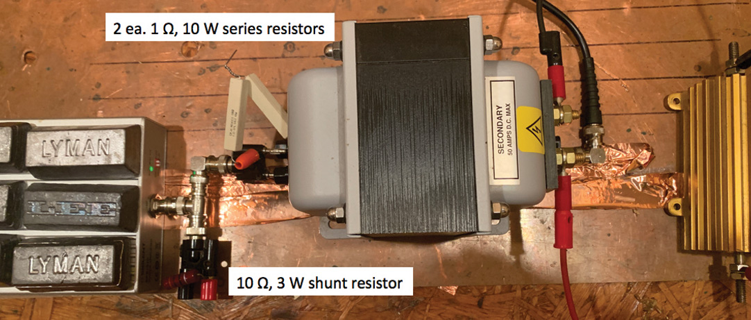
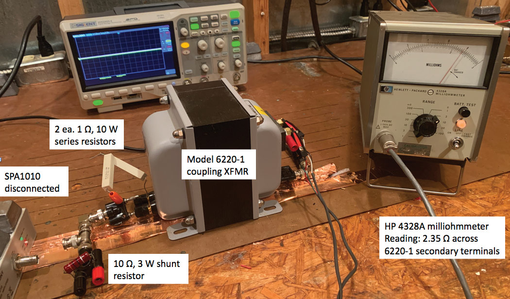
Figure 1 shows a Siglent SPA1010 10 W dc – 1 MHz amplifier in a CS01/CS101 pre-calibration measurement (see Note 11). This amplifier has 15 kΩ input impedance and very low output impedance (specified to be less than 2 Ω, but in fact measured closer to 10 mΩ). The SPA1010 amplifier is protected against both thermal and input/output overload and initially was quite touchy. When it shuts down to protect itself, that poses a hazard to the test article. Figure 2 shows thermal and overload problems successfully addressed, with the amplifier able to operate at full power (meaning 1 Vrms across a 0.5 Ω load, not full amplifier power) for hours at a time. This amounts to 40% of the amplifier’s total 10 W rated output.
The attenuator was designed for this specific application. Several purposes factored into the design, as follows:
- Attenuate high power output so that an error would not inject significantly more ripple into the test article than desired;
- Provide a well-behaved load for the amplifier regardless of test article impedance so that it does not nuisance trip and cause the test article to see a high impedance reflected across transformer windings; and
- Provide a low and near constant inserted transformer secondary impedance as seen by the test article.
If the limit is such as might be found in References 3–8 but the amplifier’s maximum output is much greater than 80 W, the attenuation may be based on that ratio. For this technical tip, the limit is as per reference 9 (1 Vrms) and the amplifier is capable of delivering 100 W into a 2 Ω load. Based on this and the above considerations, the attenuator was designed to symmetrically match 2 Ω on input and output and provide a nominal 9 dB attenuation. (Attenuator design details may be found in the Sidebar of this article.).
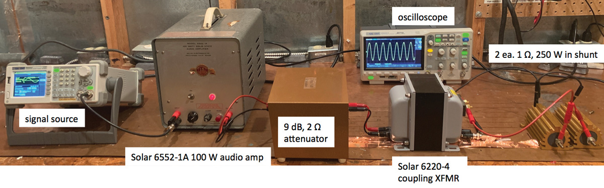
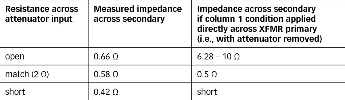
Table 1 makes it clear that the attenuator is performing the function of making impedance mismatches look much closer to an impedance match, as does any attenuator properly matched to source and load impedances.
- MIL-STD-462 CS01, Measurement of Electromagnetic Interference Characteristics, 31 July 1967.
- MIL-STD-462D CS101, Measurement of Electromagnetic Interference Characteristics, 11 January 1993.
- MIL-STD-461E-G CS101, Requirements for the Control of Electromagnetic Interference Characteristics of Subsystems and Equipment, 1999 – present.
- MIL-STD-461 basic/A CS01, Electromagnetic Interference Characteristics Requirements for Equipment, 1967 – 1980.
- MIL-STD-461 B/C CS01, Electromagnetic Emission and Susceptibility Requirements for the Control of Electromagnetic Interference, 1980 – 1993.
- RTCA/DO-160 basic-G Section 18, Environmental Conditions and Test Procedures for Airborne Equipment, 1975 – present.
- SAE J1113/2, Electromagnetic Compatibility Measurement Procedures and Limits for Vehicle Components (Except Aircraft)—Conducted Immunity, 15 Hz to 250 kHz—All Leads, 1996 – 2010.
- ISO 11452-10, Immunity to conducted disturbances in the extended audio frequency range, 2009 – present.
- AIAA S-121 8.8, Electromagnetic Compatibility Requirements for Space Equipment and Systems, 2009 – present.
- Javor, Ken, “EMC Archaeology, Uncovering a Lost Audio Frequency Injection Technique,” In Compliance Magazine, April 2011.
- https://siglentna.com/product/spa1010-10-watt-amplifier
- Lead ingots are used for a variety of purposes at the EMCC test facility, and thus were a handy solution. Any technique that removes enough heat is suitable.

- Attenuate high power output so that a test operator or software error would not inject significantly more ripple into the test article than desired;
- Provide a well-behaved load for the amplifier regardless of test article impedance so that it does not nuisance trip and cause the test article to see a high impedance reflected across transformer windings; and
- Provide a low and near constant inserted transformer secondary impedance as seen by the test article.
Based on these concerns, a 100 W amplifier and a 1 Vrms limit across 0.5 Ω, the attenuator was designed to provide a bidirectional symmetrical match to 2 Ω and attenuate so that it could provide an output of 2.5 V across 2 Ω when a 50 W power amplifier with an output impedance of 2 Ω was driving it (~12 dB). 9 dB was selected to allow 3 dB headroom. Because the amplifier was actually rated for 100 W mid-band (1 kHz), a fuse was incorporated in order to avoid having to choose attenuator component ratings for the higher power.
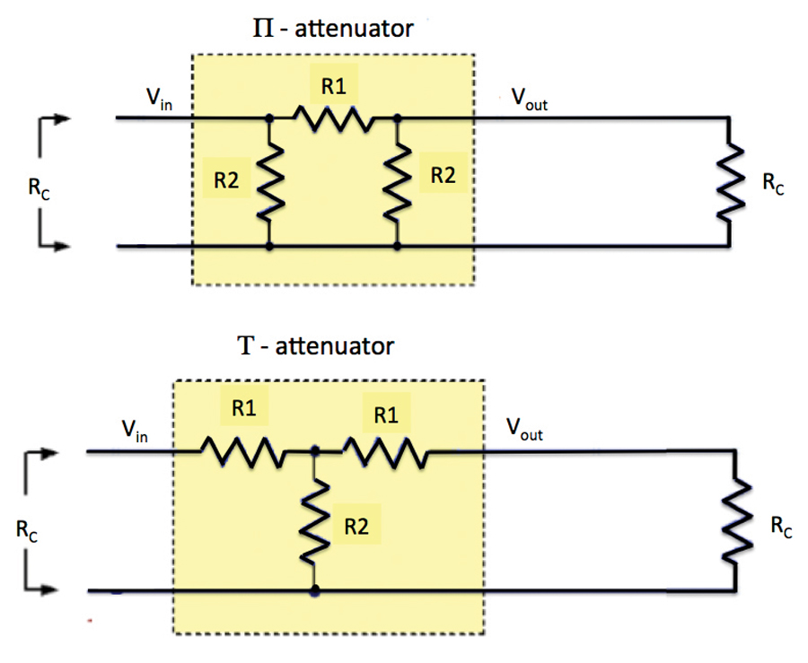
The only other design consideration is whether a symmetrical “π” or “T” configuration will be chosen. Figure 6 shows π- and T-circuit configurations.
The equations that define the resistor values in Figure 6 in the general case are:
∏-circuit: R1 = RC (1 – α2) / 2α, R2 = RC (1 + α)/(1 – α)
T-circuit: R1 = RC (1 – α) / (1 + α), R2 = RC • 2α /(1 – α2)
where
RC = impedance to match (in our audio case, 2 Ω), &
α = desired attenuation (in our case, 2.5/7 = 9 dB)
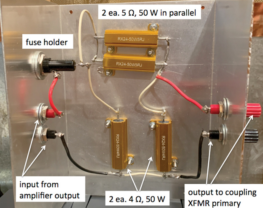
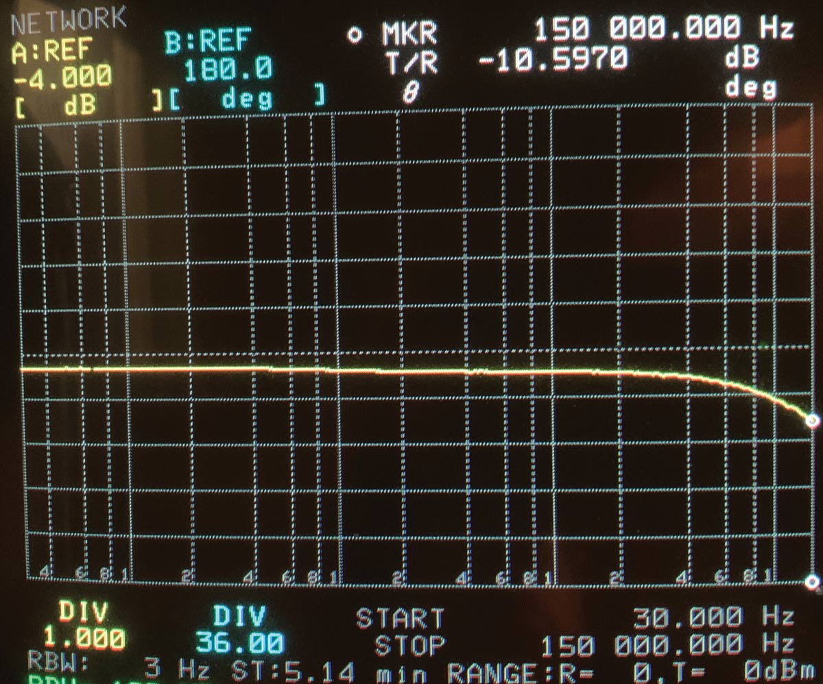
Figure 7 shows a “π” circuit realization with 4 Ω series resistance and 2.5 Ω shunt resistances. Figure 8 shows high-frequency roll-off due to the use of wire-wound high-power resistors. This could have been avoided using non-inductive resistors, at the expense of much greater assembly complexity.
It is important to note that, if the amplifier output impedance is much lower than 2 Ω, then either the attenuator input stage must include the difference, or it must be added externally in series between the amplifier output and attenuator input. Of course, if one is willing to design an attenuator for a specific amplifier, one could match the amplifier’s output resistance while retaining the attenuator’s output resistance matching to 2 Ω. In that case, the design equations in this sidebar would need to be modified accordingly.

He can be reached at ken.javor@emccompliance.com.