n Part 1 of this two-part article (see In Compliance Magazine, December 2024), we discussed the challenges involved in designing, building, and debugging a high-power mixed-signal inverter, and examining common application-specific integrated circuits (ASICs) that work alongside FETs (field effect transistor) and MCUs, focusing on their roles in interfacing and driving. In Part 2, we’ll discuss the importance of choosing the correct PCB stack up during component selection and placement, as well as component and layout mitigation strategies.

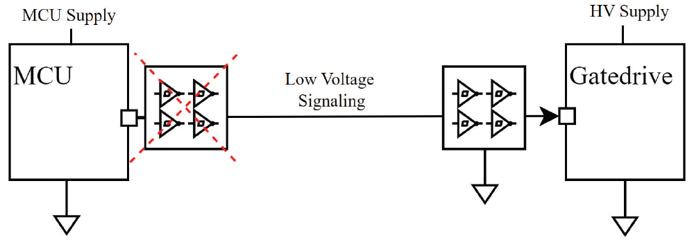
- Operating temperature of the buffer since, the warmer the inverter gets due to its proximity to the output stage of the device, the greater the likelihood that the operating point will shift;
- Ensuring that the propagation delay from input to output does not impact the functionality of the drive signal or the communication bus;
- Verifying that the VIH and VIL thresholds are compatible with your gate driver IO voltage and sufficiently high to provide immunity from stray transients; and
- Paying attention to the type of signal being buffered or level shifted. A driven IO signal, such as SPI or a low-side gate drive input, does not require a pullup resistor like I2C.
As for placement, it depends upon the type of crosstalk you’re getting since you’re looking to utilize the higher VIH/VIL thresholds of the buffer. You generally want to place the component close to the gate driver since any transient signals coupled onto the trace will have a harder time coupling (see Figure 2). Placing it near the MCU can leave the trace as an antenna, which is less effective.

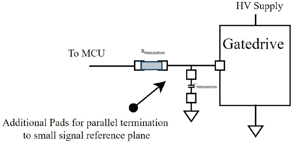
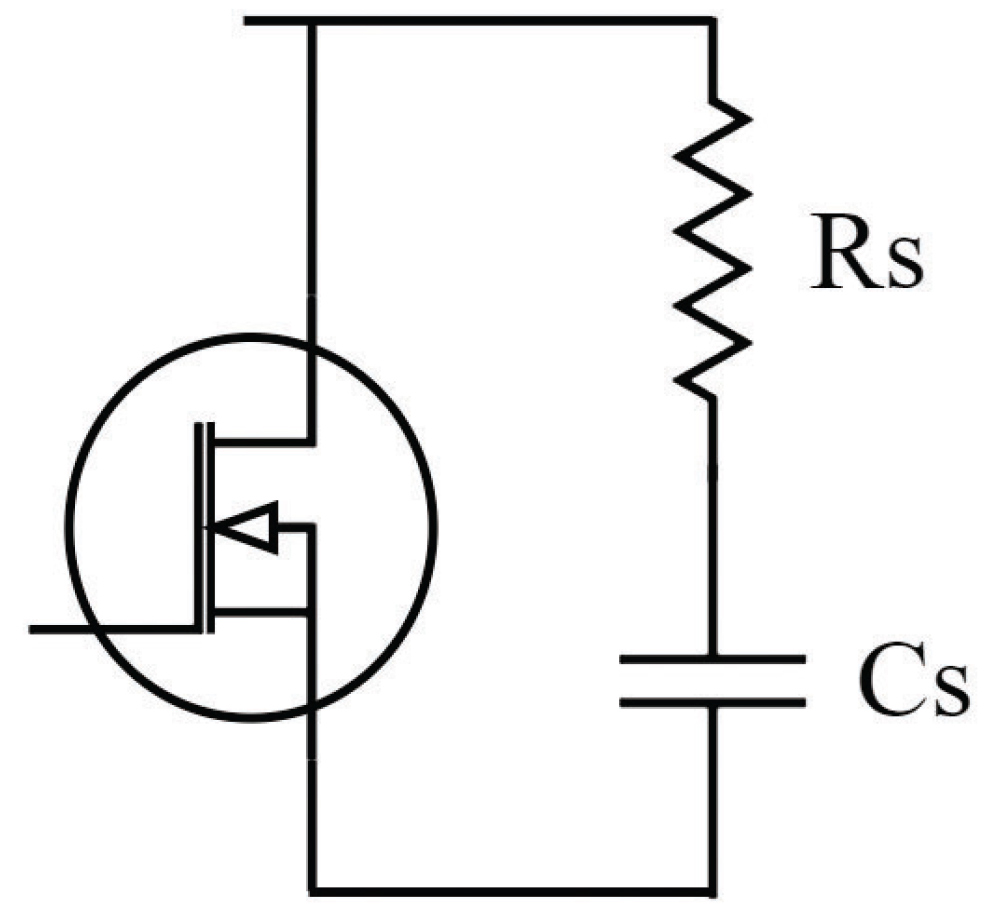
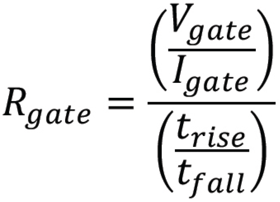
While managing noise on the victim’s side is effective, addressing the high voltage side is equally important. Designers can use two main techniques to protect against transients: snubber circuits and slowing down the edge rate (either through drive strength modifications of the gate drive strength; or a physical resistance in the gate path).
Application notes typically recommend starting with a small resistor (e.g., 10-20 ohms) and adjusting based on performance, both EMI (electromagnetic interference) and efficiency. In addition, the designer can choose the drive strength, usually represented as either percentages (the appropriately named fast/nominal/slow) or in amps.
- Increased deadtime—Slowing down the gate drive signal increases the need for deadtime, resulting in more off-time and reduced efficiency; and
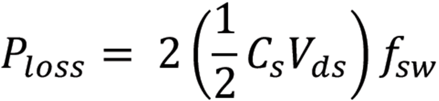
- Power dissipation—Snubbing the drive signal to reduce ringing dissipates energy as heat in the resistor-capacitor combination. The power dissipation in the snubber resistor can be significant and must be considered in thermal management planning.
Next, we’ll explore stack up, routing and grounding.
- A complete assembly usually focuses on including as much reference plane as possible to ensure proper heat and to meet rigidity concerns;
- The power levels that the assembly supports on both the input DC bus and the output generally requires “fingers” around each phase connection on exposed layer power planes to support the higher currents necessary; and
- Depending on circuitry needed for communication and logging, the fanouts and low voltage traces are limited to drive traces, CAN or ethernet communication, and sensors.
With that said, the options to consider in a design include the number of layers and planes, the ordering of those layers, and the spacing between the layers. Considering these design constraints, we can define the following traditional objectives when deciding on a stack up to help shield your sensitive traces from high voltage ones and to help with component placement:
- A signal layer should always be adjacent to the plane;
- Signals should be routed adjacent to the plane in which the components are referenced, which often results in the use of two reference planes;
- When a power plane is used, it should be placed close together to a reference plane;
- When possible, use reference layers to sandwich traces you want to either shield or keep from radiating; and
- Using more than one reference plane is very advantageous in design as it provides shielding and low impedance.

If the goal is to create tighter signal coupling between adjacent layers of the same signal type, the design then makes the interlayer spacing between these two groups thicker to allow for more isolation. An example of this is shown in Figure 7.

The answer to this question is to first identify the component categories, and thus their associated traces, and separate them into high and low voltage. By doing this, we keep a twofold goal in mind, first to keep high-power circulating return currents away from low voltage victim traces and, second to ensure a low impedance return path for those currents, preventing noise voltages from coupling onto victim traces.
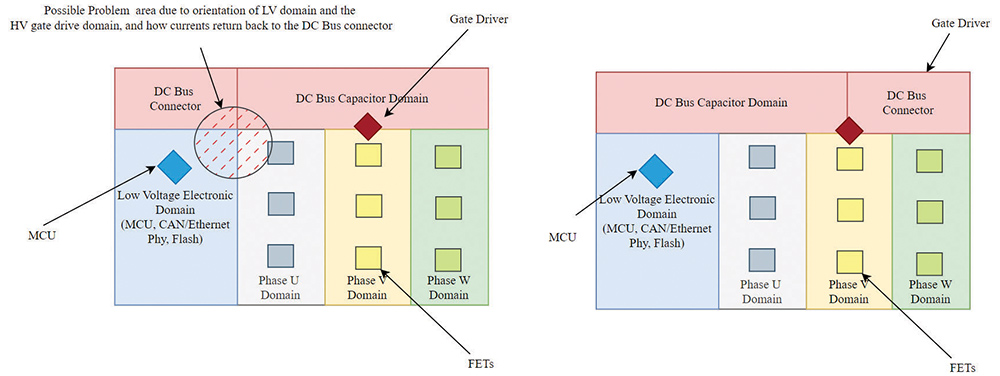
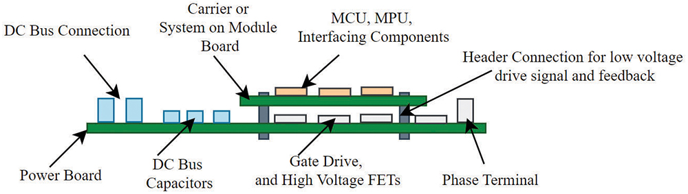
This proposed methodology splits signals into small and large signal referencing and routing planes. An example using an earlier diagram is shown in Figure 9, where we room or separate the components into high (red) and low voltage signaling (blue).

- Low voltage PWM GPIO and communication lines (I2C/SPI), which should be referenced to a plane separate from the “high power” plane, with their traces adjacent to it. Often, you’ll see terms like signal ground (s), digital ground (d), or analog ground (a) used to describe these low-voltage references. In general, they should encompass the space between the MCU and associated ASIC components (gate drives).
- Large signal referencing, which generally refers to high side PWM GPIO and their drive signals, should be referenced to a “high power” plane, where schematic symbols and pins refer this to power ground (p).
Finally, when planning for the interconnection of these various plane layers together, it’s tempting to try and galvanically isolate the high voltage switching (“noisy ground”) and low voltage (“quiet ground”) with strict adherence but often without care as to how these concepts play into the modules “system ground.”
- By galvanically isolating, or otherwise offering a single point of connection, which creates the possibility of high impedance interconnections, resulting in an increase in common mode noise voltages and currents; or
- Physical cuts in the plane, either via trace or removal of copper for galvanic isolation, which can result in an increase in radiated emissions as currents capacitively couple across the discontinuities.
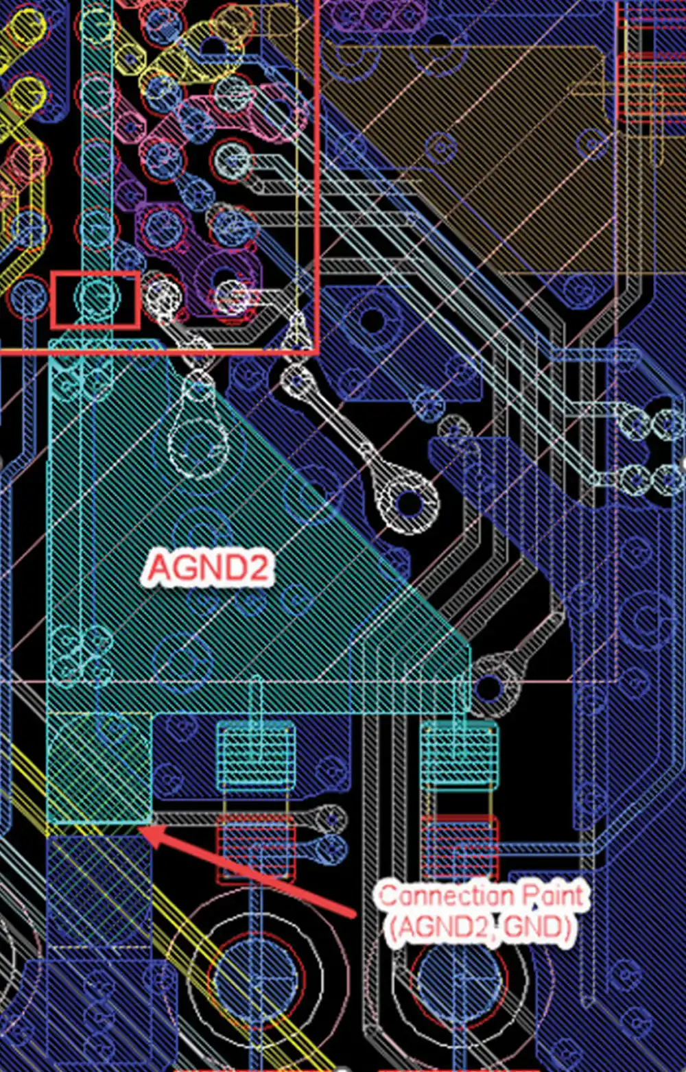
An example of a single-point connection between reference planes is shown in Figure 10, in which any electrical transients referenced to AGND but coupled onto a trace referenced to GND will have to travel back through this single-point connection.

In the last section of this article, we’ll introduce the concept of rooming as a precursor to actual design.
- Low voltage signaling—Typically made up of an MCU and supporting devices (such as flash, Ethernet or CAN PHY, and sensors), and half of the gate driver circuit.
- High voltage input section—Includes input connectors that carry the brunt of the power from the bus voltage and the DC bus caps that stabilize the DC bus during actuation.
- High voltage switching section—Comprises various sections of the three phases, the output switches, and the other half of the gate driver.