EMC Concepts Explained
Impact of PCB Via and Trace Geometry on the Effectiveness of Decoupling Capacitors
Part 2: Conducted Emissions Results – Impact of the Distance Between the Capacitor and IC
T

his is the second article in the series investigating the effectiveness of decoupling capacitors while varying the topology of vias, trace length between the decoupling capacitor and the IC power/ground pins, and distance from the internal power-ground plane pair. The first article, [1], introduced the PCB schematic, via and trace topologies, as well as PCB topology. This article addresses the impact of the distance of the capacitor from the IC on the conducted emissions. The IC used in the PCB design is the PIC10F200 from Microchip. This IC has an internal clock frequency of 4 MHz.

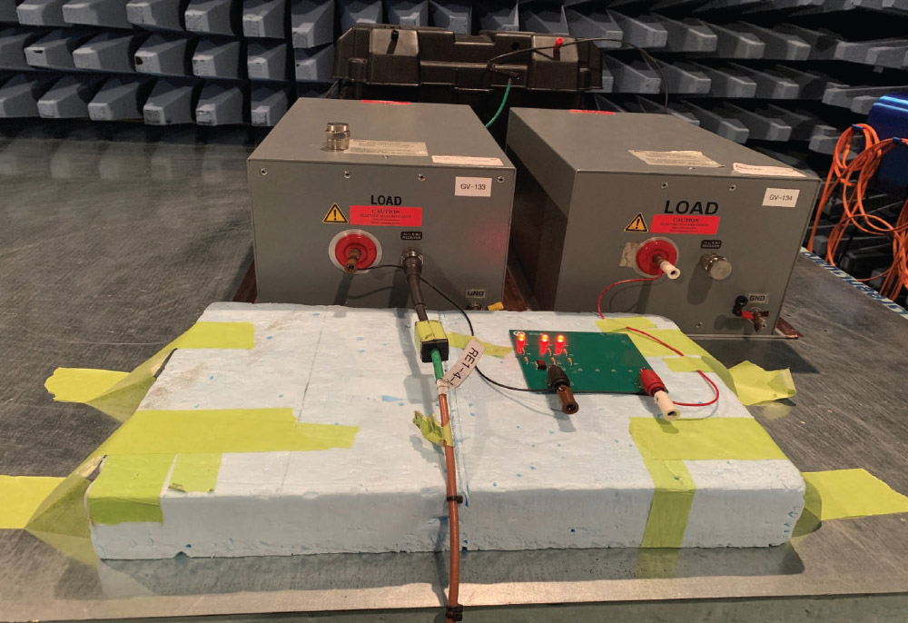
The RF Conducted Emissions of the PCB assemblies were measured on the external Power and Ground lines using the CISPR 25 (CE Voltage Method) standard setup with two Line Impedance Stabilization Networks (LISN). For the purposes of simplifying the study, the majority of the plots shown are for the Power (Battery) line. When power is applied to the IC, it toggles the LEDs on and off, rapidly using a constant rate. The purpose of switching the LEDs on and off rapidly is to create a periodic power (charge) draw, thus creating a need for proper Power Delivery Network (PDN) decoupling to reduce or eliminate conducted and radiated emissions. Note that the IC technology used in this design is bandwidth limited and its maximum edge rates and clock speed are rather slow compared to most high‑speed technologies. Therefore, there is a limit to the frequency bandwidth over which this particular IC can generate emissions from its PDN structure, and this in turn limits the frequency span over which this study is evaluated.

Project Overview
Figure 1 shows the block diagram of the system studied, together with the via configurations and the capacitor placements.
Figure 1: a) system block diagram, b) via configurations, c) capacitor placement
One bank of capacitor pads (C1 through C7) is located on the top layer of the PCB, and the other bank of pads (C8 through C14) is placed on the bottom layer of the PCB, at the same distances from the microprocessor (see [1] for more details). Only one pad at a time was populated with a 0.1 µF X7R capacitor. The capacitor value was chosen based on the recommended value from the manufacturer’s datasheet.
The 6-layer PCB used in our study is shown in Figure 2. Six PCBs were tested, each with a different via topology, as shown in Figure 1b. Board 4 differs from the other boards, not only with a via topology but also by having a long trace connected to the power pin of the IC. There is no via from the capacitor to the power plane, unlike all other boards.

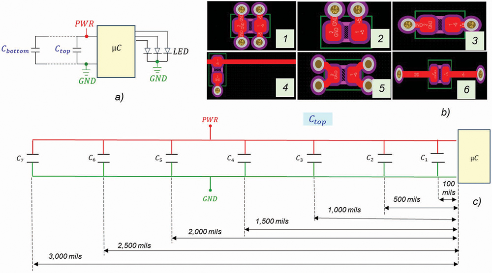
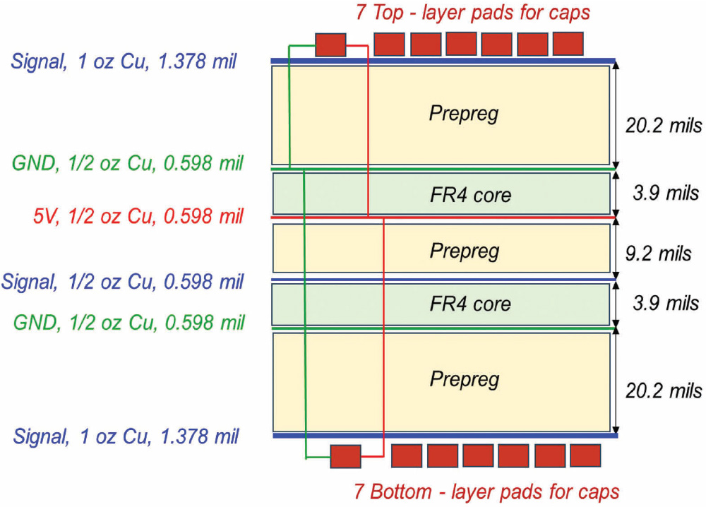
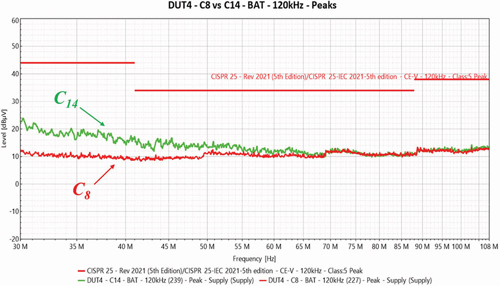
As Figure 2 shows, the top layer capacitors were closer to the internal power-ground plane pair than when placed on the bottom layer.

Figure 2: Topology of the 6-layer PCB
In summary, the via topology, capacitor distance from the IC, and capacitor distance from the power-ground pair were varied.
Conducted Emission Measurement Setup
The measurement setup according to CISPR 25 specification is shown in Figure 3.
Figure 3: Measurement setup for conducted emissions
Measurements in frequency range 0.15 – 30 MHz were performed with 9 kHz resolution bandwidth (RBW), while the range 30 – 108 MHz used 120 kHz RBW. Emissions were evaluated against Class 5 limits using the peak, average, and quasi‑peak detectors.
Conducted Emission Results – Effect of the Distance Between Capacitor and IC
The effect of the distance between the capacitor and the IC was most pronounced for board 4. In the frequency range 0.15 – 30 MHz for the top side of the board, the emission results showed similar trends as the distance increased from C1 to C7. Figure 4 shows the results on the battery line for the C1 versus C7 locations.
Figure 4: 0.15 – 30 MHz, top side of Board 4 PCB: C1 vs. C7 locations
Both configurations show failures below 2 MHz but a comparison of the plots shows a few decibel (dB) increase in emissions by moving the capacitor from the location closest to the IC (C1) to the farthest (C7) on the top side of the PCB. The results for the bottom side of the board in the same frequency range 0.15 – 30 MHz showed a similar trend, shown in Figure 5.
Figure 5: 0.15 – 30 MHz, bottom side of PCB: C8 vs. C14 locations
In the frequency range 30 – 108 MHz, the results for the top side of the board were virtually identical (and similar to the ambient measurement), as the distance increased from C1 to C6. However, the results for the C7 location were significantly different. Figure 6 shows the results on the battery line for the C1 versus C7 locations. A comparison of the graphs indicates that the IC is sufficiently decoupled to address the conducted emissions in this upper band when the capacitor is placed in the C1 location. However, when the capacitor location is moved to the position farthest away from the IC, the PDN is insufficiently decoupled, and this gives rise to a significant increase in conducted emissions. This is likely due to the additional inductance in the increased loop area established by the flow of current in the circuit.
Figure 6: 30 – 108 MHz, top side of PCB: C1 vs. C7 locations
The emissions for the location at C1 were well below the peak detector limit and similar to ambient measurements, whereas the results for the C7 location were significantly higher, particularly around 55 MHz.

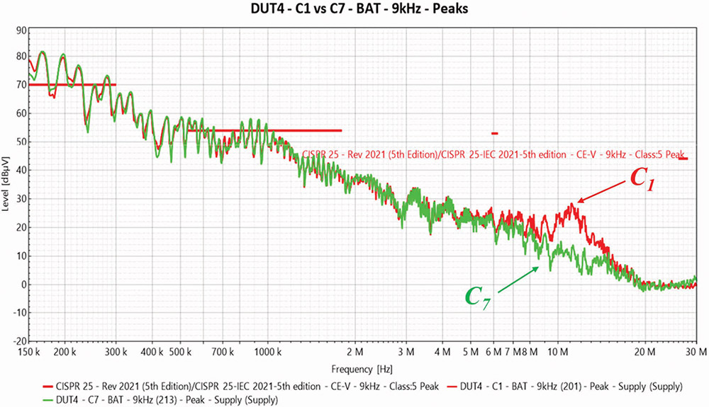
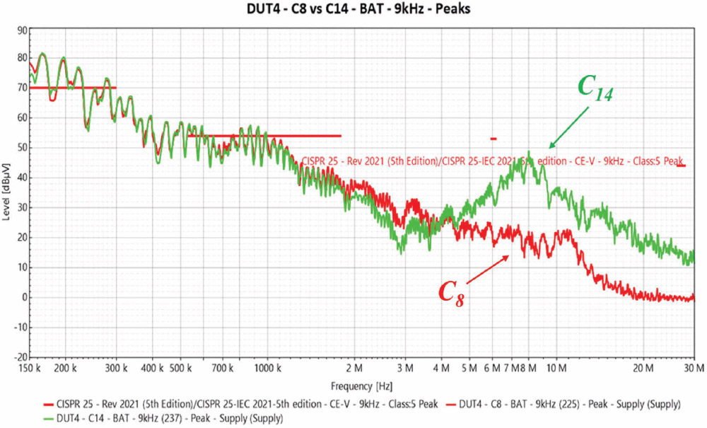
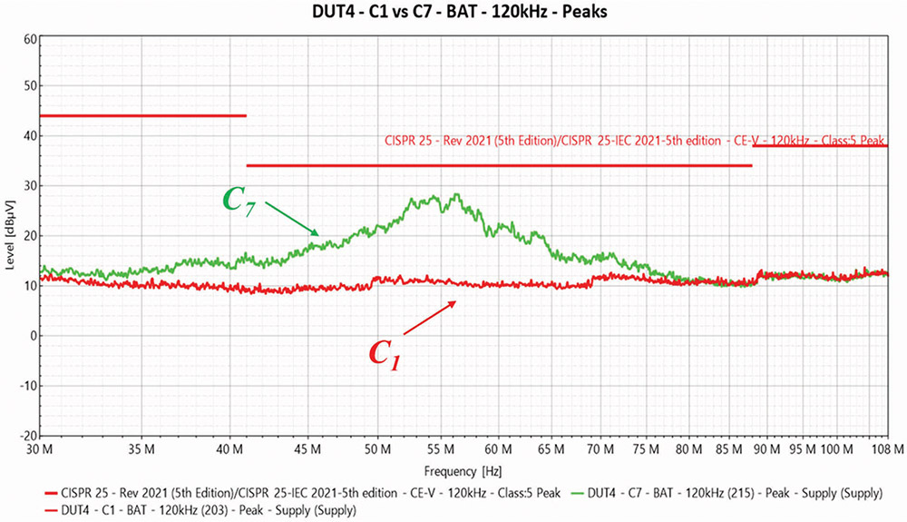
In the frequency range 30 – 108 MHz, the results for the case with the decoupling capacitor placed on the bottom side of the board showed an increase in conducted emissions over a different frequency range. Figure 7 shows the results on the battery line for C8 (location closest to the IC) versus C14 (location farthest from the IC).

Figure 7: 30 – 108 MHz, bottom side of PCB: C8 vs. C14 locations
While the conducted emissions did not exceed the class 5 limits, the emissions did increase below 60 MHz when the capacitor was moved from the C7 location to the C14 location.
Future Article
The next article will present the impact of the distance from the power-ground plane pair and the impact of via topology on the conducted emission.
Reference
  1. Bogdan Adamczyk, Allyson Telck, Scott Mee, “Impact of PCB Via and Trace Geometry on the Effectiveness of Decoupling Capacitors – Part 1: Board Topologies and the PCB Circuitry,” In Compliance Magazine, February 2026.
Share this story:
Dr. Bogdan Adamczyk
The Authors
Dr. Bogdan Adamczyk is professor and director of the EMC Center at Grand Valley State University (http://www.gvsu.edu/emccenter) where he performs EMC educational research and regularly teaches EM/EMC courses and EMC certificate courses for industry. He is an iNARTE-certified EMC Master Design Engineer. He is the author of two textbooks, “Foundations of Electromagnetic Compatibility with Practical Applications” (Wiley, 2017) and “Principles of Electromagnetic Compatibility: Laboratory Exercises and Lectures” (Wiley, 2024). He has been writing “EMC Concepts Explained” monthly since January 2017. He can be reached at adamczyb@gvsu.edu.
Allyson Telck
Allyson Telck is participating in a combined degree program to earn a Bachelor of Science in Electrical Engineering and a Master of Science in Biomedical Engineering at Grand Valley State University. She recently completed her final rotation as an Electromagnetic Compatibility Engineering co‑op student at E3 Compliance, which specializes in EMC and high-speed design, pre‑compliance testing, and diagnostics. She can be reached at allyson.telck@e3compliance.com.
Scott Mee
Scott Mee is a co-founder and owner at E3 Compliance, which specializes in EMC & SIPI design, simulation, pre-compliance testing, and diagnostics. He has published and presented numerous articles and papers on EMC. He is an iNARTE certified EMC Engineer and Master EMC Design Engineer. Mee participates in the industrial collaboration with GVSU at the EMC Center. He can be reached at scott.mee@e3compliance.com.