Documents Can Be Your Friend or Foe
EMC Concepts Explained
Hot Topics in ESD

Documents Can Be Your Friend or Foe
EMC Concepts Explained
Hot Topics in ESD

ISSN 1948-8254 (print)
ISSN 1948-8262 (online)
is published by
Same Page Publishing Inc.
451 King Street, #458
Littleton, MA 01460
tel: (978) 486-4684
fax: (978) 486-4691
© Copyright 2026 Same Page Publishing, Inc. all rights reserved
Contents may not be reproduced in any form without the prior consent of the publisher. While every attempt is made to provide accurate information, neither the publisher nor the authors accept any liability for errors or omissions.
editor-in-chief
Please contact our circulation department at circulation@incompliancemag.com

A Report and Order issued by the Commission adopted new rules that will provide access to all 10 megahertz of the 900 MHz band. This action will reportedly enhance spectrum capacity to address the growing demand for private and secure wireless broadband networks serving utilities, critical infrastructure, and enterprise businesses…
According to a press release issued by the Commission in early February, TikTok features such as autoplay, push notification, and its personalized recommender system are addictive and “could harm the physical and mental well-being of its users, including minors and vulnerable adults…
But Why Though?
here’s a lot of EMC testing that focuses on the 30 MHz to 1 GHz range, specifically radiated emissions tests like FCC/ANSI C63.4 or CISPR 25. There are plenty of requirements that go up from there (up to 18 GHz for MIL-STD-461 RE102 testing or 40 GHz if you’re really unlucky), and some that go down from there, such as the conducted emissions 150 kHz – 30 MHz test for FCC/ANSI C63.4. But then there are some tests that look at the 9 kHz – 30 MHz range specifically in radiated terms, like CISPR 36 taking measurements from 150 kHz – 30 MHz using loop antennas. In these standards, limits are written in A/m for magnetic fields instead of the V/m electric fields we’re all more used to. Why?
It all comes down to the difference between the “near field” and “far field”. (For a lot more detail on this topic, see Ken Javor’s four-part series on near field measurements in this very magazine, starting here.) We think of electromagnetic waves as being very consistent over space. If we measure only the electric field (E-field) coming from a device under test (DUT), then we’ll get good information about both the electric and magnetic fields (H-field) associated with the unit. This works because the H-field and E-field are related to each other by the wave impedance number, which is a constant (120π or 377Ω). But this is only true if you are taking your measurement in the far field distance from the DUT.
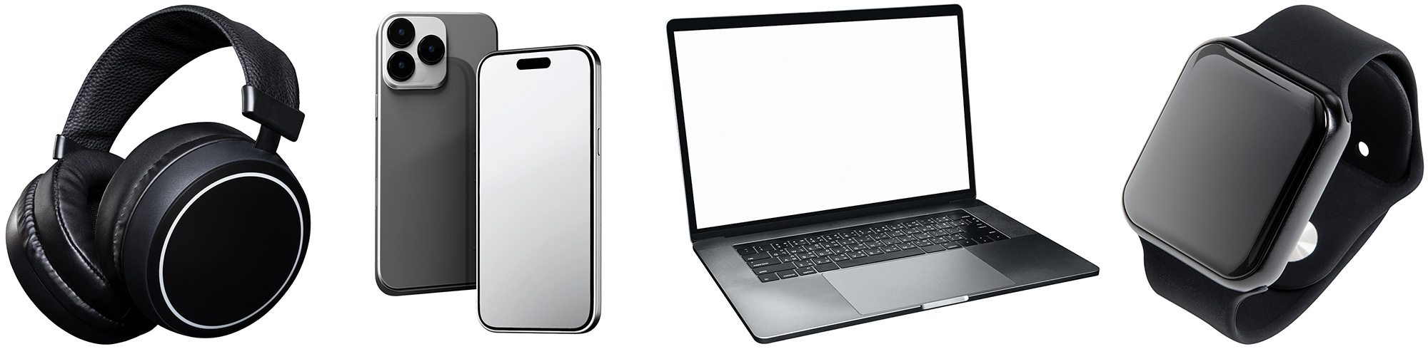
nsuring electromagnetic compatibility (EMC) in consumer electronics is complex yet essential. The proliferation of electronic devices in our daily lives has increased the potential for electromagnetic interference (EMI), which can disrupt device functionality and affect user experience. This article delves into the challenges faced in designing for EMC compliance, explores effective design strategies, and highlights successful case studies.
- Miniaturization: As devices become smaller, the proximity of components increases, leading to higher chances of interference. The compact design limits the space for adding shielding and other EMC mitigation techniques.
- High-Frequency Operation: Modern devices often operate at high frequencies to achieve faster data transfer and better performance. Higher frequencies are more susceptible to EMI, making it crucial to design circuits that can handle these frequencies without compromising EMC.

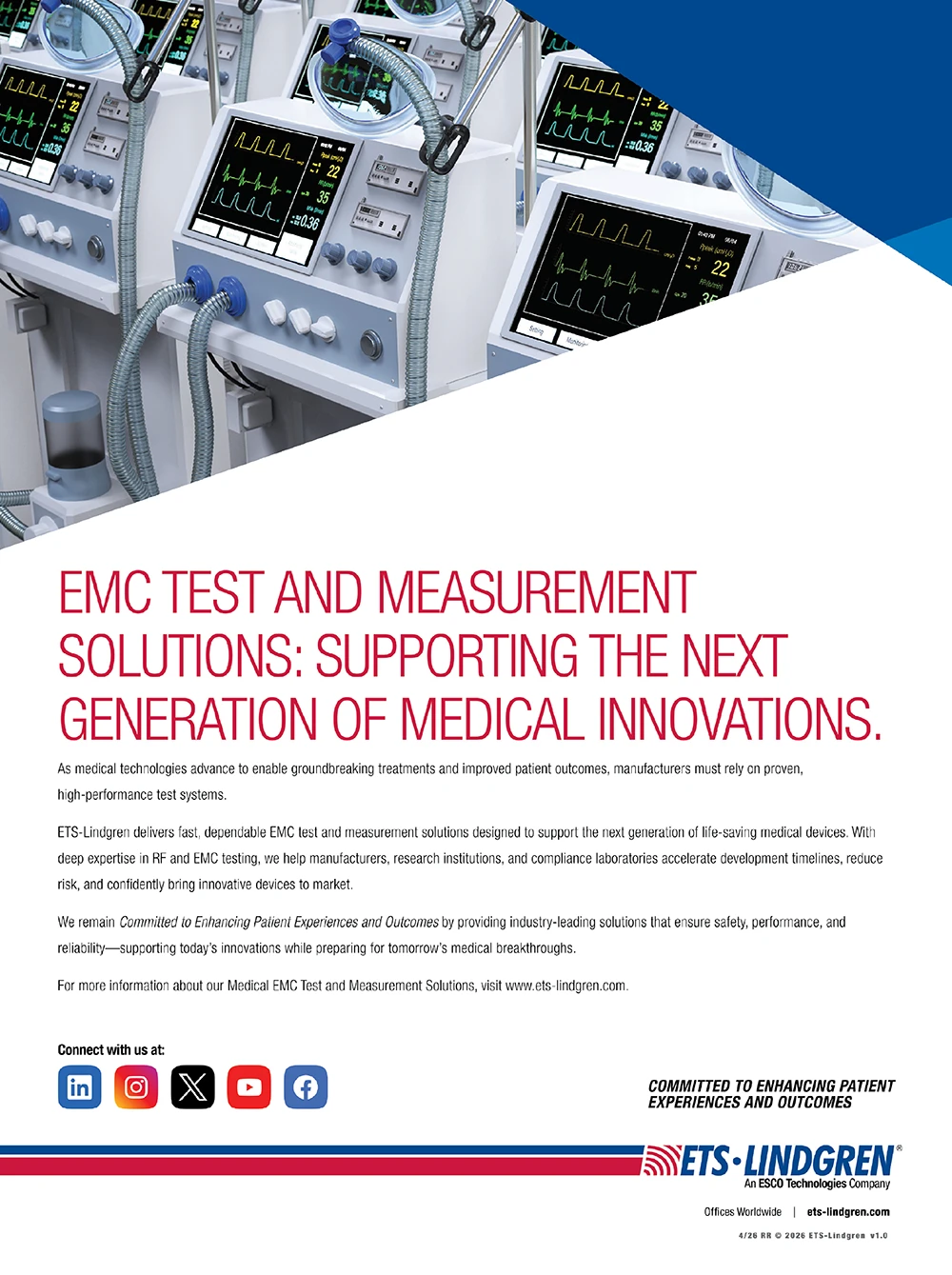
of new certification projects fail to comply with the minimum requirements of published medical safety and performance standards. This article explores some of the major challenges faced by medical device designers and manufacturers when asked by local authorities, regulatory bodies, government agencies, or other sources to demonstrate evidence of compliance with applicable medical standards. Whether it’s to support a U.S. FDA 510(k) submission, European Union Regulation (EU) 2017/745, Brazil’s ANVISA, China’s NMPA, sale to hospitals and healthcare professionals, or a device manufacturer’s own internal verification and validation efforts, safety and performance standards come into play.
The majority of issues that third-party test labs and certification agencies encounter stem from:
- Lack of awareness and application of all relevant standards throughout the design process;
- Waiting until “design freeze” to partner with a knowledgeable, accredited third-party test lab or certification agency;
- Being unprepared for standard evaluations without sufficient evidence to demonstrate compliance (including production-equivalent samples, complete user manuals, product labeling/markings, accurate isolation schemes, critical component lists with traceability to component-level approvals, having a compliant quality system, missing or incomplete supporting documentation, etc.);


EC 60601 is a family of internationally accepted standards that serve as the primary safety standards for medical electrical equipment, software, and systems used around the world. IEC 60601 standards are prepared and maintained by Technical Committee 62 (TC62) of the International Electrotechnical Commission (IEC ). The General standard and related Collateral standards are prepared and maintained by IEC subcommittee 62A – Common aspects of medical equipment, software, and systems.


ocuments, including electronic records, are extremely important to any manufacturer, distributor, or retailer. While employees come and go and change jobs within an organization, the design plans, engineering drawings, production procedures, safety memoranda, and marketing strategies they have created represent a historical record of the safety that a manufacturer included in the product. These documents can significantly help or hurt a manufacturer or product seller, especially in the event of product liability litigation.
Unfortunately, no one knows whether an organization’s documentation will help or hurt until a lawsuit is brought or the U.S. Consumer Product Safety Commission (CPSC) initiates an investigation and the manufacturer has to produce documents requested by the plaintiffs or the CPSC. In addition, there may be documents that could be helpful, but which were written in a way that could possibly benefit the plaintiffs. And, perhaps even more frustrating, there may also be documents reflecting safety activities that were created but then destroyed before litigation or an investigation arose.
his is the second article in the series investigating the effectiveness of decoupling capacitors while varying the topology of vias, trace length between the decoupling capacitor and the IC power/ground pins, and distance from the internal power-ground plane pair. The first article, [1], introduced the PCB schematic, via and trace topologies, as well as PCB topology. This article addresses the impact of the distance of the capacitor from the IC on the conducted emissions. The IC used in the PCB design is the PIC10F200 from Microchip. This IC has an internal clock frequency of 4 MHz.
The RF Conducted Emissions of the PCB assemblies were measured on the external Power and Ground lines using the CISPR 25 (CE Voltage Method) standard setup with two Line Impedance Stabilization Networks (LISN). For the purposes of simplifying the study, the majority of the plots shown are for the Power (Battery) line. When power is applied to the IC, it toggles the LEDs on and off, rapidly using a constant rate. The purpose of switching the LEDs on and off rapidly is to create a periodic power (charge) draw, thus creating a need for proper Power Delivery Network (PDN) decoupling to reduce or eliminate conducted and radiated emissions. Note that the IC technology used in this design is bandwidth limited and its maximum edge rates and clock speed are rather slow compared to most high‑speed technologies. Therefore, there is a limit to the frequency bandwidth over which this particular IC can generate emissions from its PDN structure, and this in turn limits the frequency span over which this study is evaluated.
his column is the third in a three-part series on testing small form factor products for CDM. Part 1 highlighted the issues of CDM testing with the current field-induced CDM (FICDM) testers. The main problems are first the pogo pin size vs package or ball bump size and second small form factor products may have very low withstand voltages where the FICDM testers are known to be unreliable. Part 2 highlighted solutions that were still air discharge. In Part 3, solutions where contact to the part is made first and then a stress similar to a CDM stress is applied. These solutions are not air discharge.


View Index
You can do that here.