his column is the third in a three-part series on testing small form factor products for CDM. Part 1 highlighted the issues of CDM testing with the current field-induced CDM (FICDM) testers. The main problems are first the pogo pin size vs package or ball bump size and second small form factor products may have very low withstand voltages where the FICDM testers are known to be unreliable. Part 2 highlighted solutions that were still air discharge. In Part 3, solutions where contact to the part is made first and then a stress similar to a CDM stress is applied. These solutions are not air discharge.
Figure 1 depicts a possible setup for CC-TLP. The DUT is placed on the chuck of a wafer prober. The VF-TLP system generates the pulse, which passes the pick-off for the pulse voltage measurement and is then injected into a 50-ohm transmission line. The transmission line’s ground shield connects to the ground plane and the signal line is connected to a probe needle, which connects to the DUT through a small hole in the ground plane. The voltage and current flowing at the DUT pin as a function of time can be calculated from the sum and difference of the incident and reflected pulses.
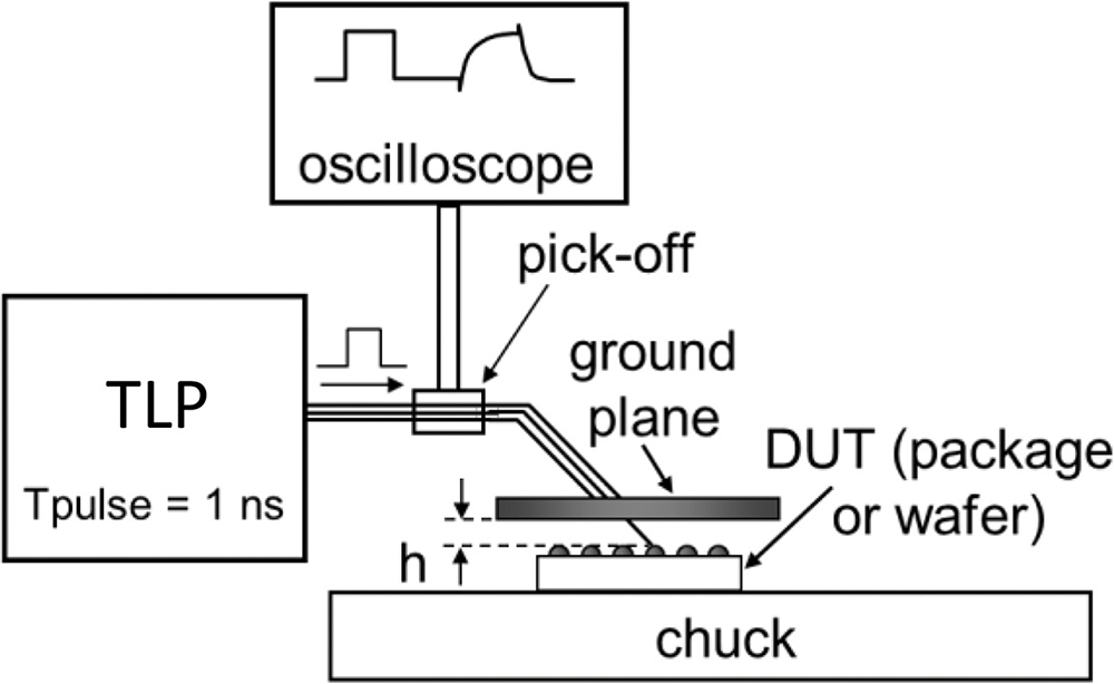
Many studies exploring 3 µm to 7 nm technologies have demonstrated the excellent correlation of CC‑TLP with CDM in terms of stress current failure threshold as well as electrical failure and physical damage signature [3][4][5].
The connection to the pogo pin is very different in LI‑CCDM than in field-induced CDM. Figure 2 shows a diagram of an LI-CCDM system. The coupling plane is the field plate from ANSI/ESDA/JEDEC JS‑002, but it is tied to ground with the isolation resistor rather than charged to a high voltage. The ground plane size is also the same as in ANSI/ESDA/JEDEC JS-002, and it has a similar pogo pin for contacting the device being tested.
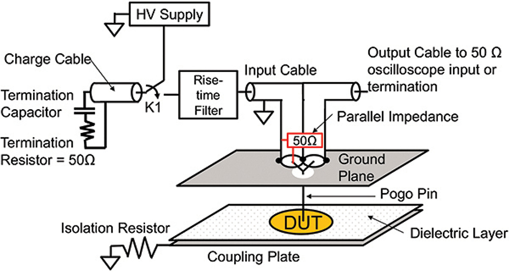
- The field plate is at ground potential with the assumed neutrally charged die on the field plate.
- The relay is closed to ensure the probe tip is at zero potential before contact with the DUT.
- The probe tip is brought into contact with the pin under test.
- The relay is opened.
- The field plate is slowly raised to a high potential, capacitively coupling the DUT to a high potential.
- The relay is closed, initiating the discharge.
These are all viable options for bare-die CDM testing. There is no consensus on which one of these options is the best. The three-part column is an attempt to introduce the issues with testing small form factor parts at low CDM withstand voltages and offer solutions to these problems.
- H. Wolf, H. Gieser, W. Stadler and W. Wilkening, “Capacitively Coupled Transmission Line Pulsing CC‑TLP – A Traceable and Reproducible Stress Method in the CDM-Domain,” Journal of Microelectronics Reliability, Elsevier, volume 45, no. 2, 2005.
- H. Gieser, H. Wolf, and F. Iberl, “Comparing Arc‑free Capacitive Coupled Transmission Line Pulsing CC-TLP with Standard CDM Testing and CDM Field Failures,” Tagungsband 9, ESD‑Forum Berlin 2005.
- H. Wolf, H. Gieser, K. Bock, A. Jahanzeb, C. Duvvury, and Y. Lin, “Capacitive Coupled TLP (CC‑TLP) and the Correlation with the CDM,” EOS/ESD Symposium 2009.
- J. Weber, H. Gieser, H. Wolf, L. Maurer, K. T. Kaschani, N. Famulok, R. Moser, K. Rajagopal, M. Sellmayer, A. Sharma and H. Tamm, “Correlation study of different CDM testers and CC-TLP,” EOS/ESD Symposium 2017.
- H. Wolf, H. Gieser, D. Walter, “Investigating the CDM Susceptibility of IC’s at Package and Wafer Level by Capacitive Coupled TLP,” EOS/ESD Symposium 2007.
- ANSI/ESD SP5.3.3 – Charged Device Model (CDM) Testing-Component Level Low-Impedance Contact CDM as an Alternative CDM Characterization Method.
- Simicic, M., Wu, W‑M., Jack, N., Tamura, S., Shimada, Y., Sawada, M., & Chen, S.-H. (2020), “Optimization of wafer-level low-impedance contact CDM testers,” EOS/ESD Symposium Proceedings 2020.
- M. Simicic et al., “Wafer-Level LICCDM Device Testing,” 2021 43rd Annual EOS/ESD Symposium (EOS/ESD), pp. 1-8, 2021.
- M. Drallmeier, L. Zeitlhoefler, H. Yang, W. Huang, F. zur Nieden, D. Pommerenke, “A Relay Discharged FICDM Method for Improved Repeatability,” EOS/ESD Symposium 2020.
- Kathleen Muhonen, “Small Form Factor CDM Testing, Part 1: Problems with FICDM Testing for Small Form Factor and Interface Die,” In Compliance Magazine, January 2026.
- Kathleen Muhonen, “Small Form Factor CDM Testing, Part 2: Air Discharge Options,” In Compliance Magazine, February 2026.

Kathleen Muhonen is a Principal Development Engineer at Qorvo, specializing in ESD protection and instrumentation. She serves on ESDA device testing standards committees and holds a Ph.D. in EE from Penn State, with prior roles at HP and Lockheed Martin.