his is the first article of a two-article series devoted to the return current distribution in a 2-layer FR-4 PCB microstrip line configuration with a solid reference plane. This topic was discussed in [1], where the analytical results for a solid reference plane were presented. In this article, we compare these analytical results to the CST Studio simulation results. Simulation results closely follow the analytical results and give an insight into the details of the return current distribution. In Part 2, we will discuss the return current distribution in the reference plane containing numerous via anti-pads (cutouts).
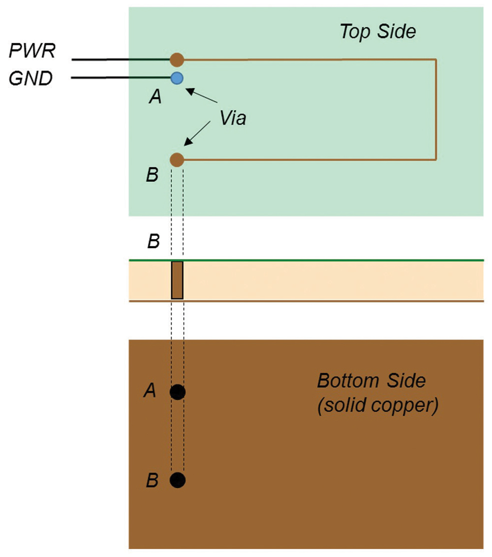
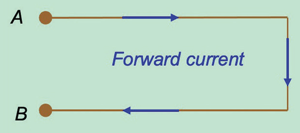
At points A and B, vias connect the top trace to the ground (reference) plane. The forward current flows on the top trace as shown in Figure 2.
Upon reaching the point B the current travels to the reference plane and returns to the source (A). Current returns to the source through the path of least impedance. At high frequencies, the return current takes the path of least inductance, which is directly underneath the forward current trace, because this represents the smallest loop area (smallest inductance).
The current distribution in the reference plane underneath the trace is described by its current density [3], J(x):
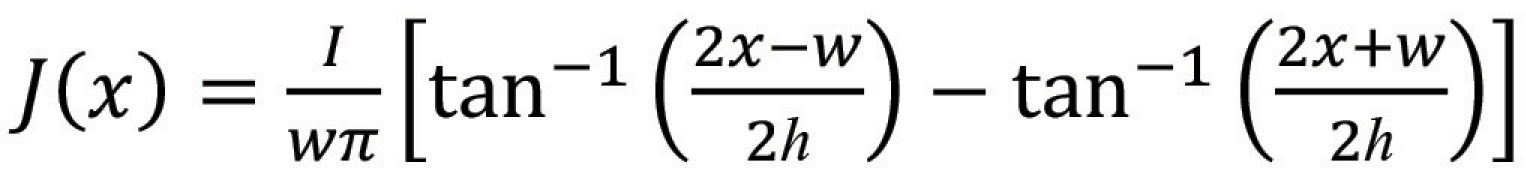
where I is the total current flowing in the loop. This formula is valid at frequencies where the resistance of the reference return plane is negligible compared to its inductive reactance. This effect will be visualized in the simulation section of this article.
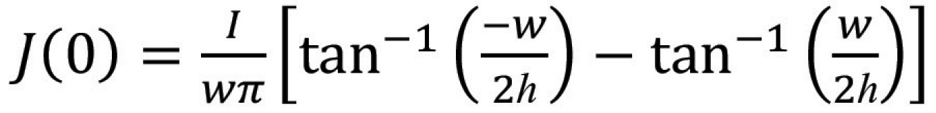
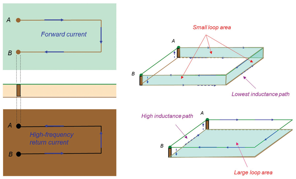
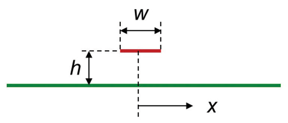
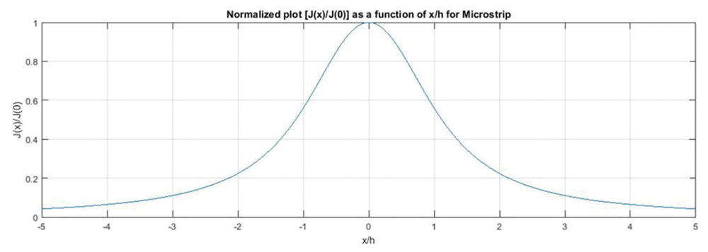
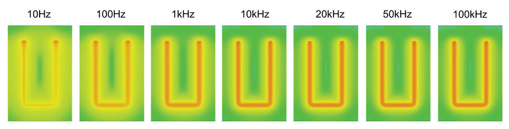
Figure 7 shows the return current path (forward current trace is hidden) flowing in the reference plane at different frequencies.
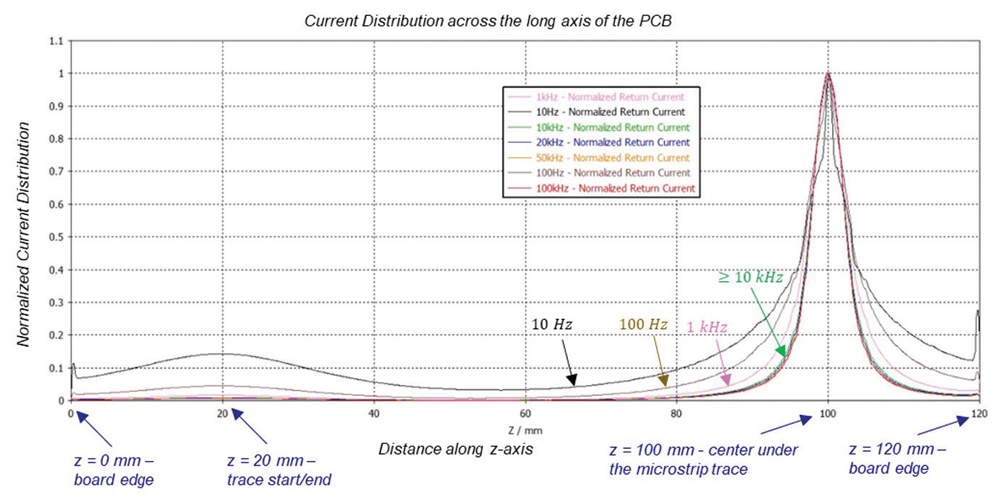
Observations: At 10 Hz the return current spreads wide over the reference plane, flowing both under the top trace and directly from the load port to the source port. As the frequency increases to 100 Hz, more of the return current flows under the trace (with a narrower spread), and less of it flows directly from the load port to the source port. This trend continues as the frequency increases to 1 kHz.
The results for 10 kHz and beyond show something very interesting. As the frequency increases beyond 10kHz, the return current path remains virtually unchanged, predominantly flowing beneath the forward trace. In other words, the return current path and current density no longer depend on frequency. The frequency is high enough that the resistance of the return plane is negligible compared to its inductive reactance, [3].
This phenomenon is explained in [4], as follows: “The current distribution, …, balances two opposing forces. Were the current more tightly drawn together, it would have higher inductance (a skinny wire has more inductance than a broad, flat one). Were the current spread farther apart from the signal trace, the total loop area between the outgoing and returning signal paths would increase, raising the inductance.”
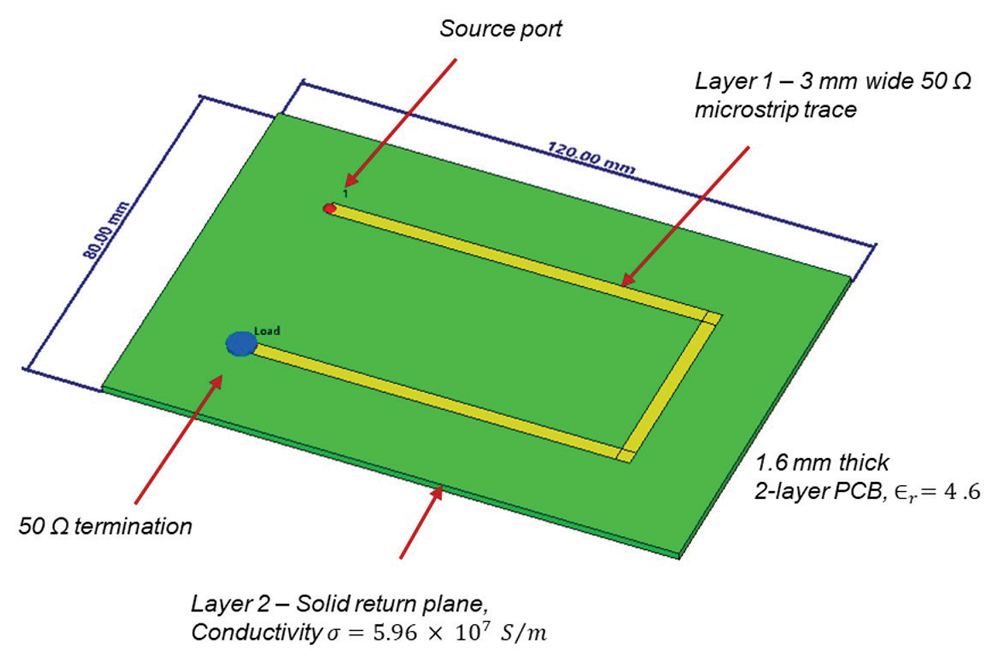
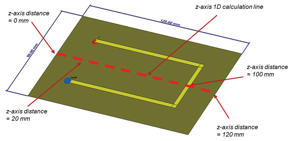
Figure 8 shows the details of the PCB simulation model used to plot the current density distribution. A straight line that cuts down the middle of the longitudinal axis of the reference plane is used to obtain the simulated magnitude of the current density.
References
- Bogdan Adamczyk, “PCB Current Distribution in a Microstrip Line,” In Compliance Magazine, November 2020.
- Bogdan Adamczyk and Jim Teune, “Alternative Paths of the Return Current,” In Compliance Magazine, May 2017.
- Henry W. Ott, Electromagnetic Compatibility Engineering, Wiley, 2009.
- Howard Johnson and Martin Graham, High‑Speed Digital Design, a Handbook of Black Magic, Prentice Hall, 1993.

