

power management integrated circuit (PMIC) is more than a collection of regulators in an integrated circuit package. It is a coordinated power system, often paired with a complex or specialized microprocessor (MPU) or system-on-chip (SoC), that typically features:
- Centralized sequencing logic to control startup and shutdown procedures;
- Fault aggregation, where faults are collected and reported in one place;
- Digital control logic, usually including a register map and watchdog logic; and
- Some form of non-volatile configurable memory that allows you, the system integrator, to match the device to the specific needs of your system.
This article focuses on the system challenges that follow PMIC selection. We will build a hierarchy that starts with load definition, specifically the complex devices that PMICs are normally placed next to, and the requirements those devices impose. From there, we will move up the abstraction tree into the power topologies normally implemented around PMICs, including primary and secondary regulator interaction and the point at which a dedicated core rail regulator is required. Finally, we will focus on features, sequencing, fault reaction, and layout-driven integration concerns.
A common industry failure mode is reversing that order: picking a PMIC because it appears on a reference design or because it advertises a desired feature set, without first proving that the rail budget, startup behavior, steady-state behavior, and shutdown behavior match the system. The consequence is usually a late-stage discovery that the part cannot meet transient droop on a CPU rail, or that the sequencing or fault recovery is not congruent with the system’s needs without a one-time programmable (OTP) revision. Both situations are avoidable with a week of paper engineering before schematic capture, using the framework this article provides.
Before selecting a PMIC or drawing a power tree, the rail requirements must be extracted from the target processor’s documentation and reformulated into a form that the power design can act on. The difficulty is that the processor datasheet is usually written from the silicon’s perspective, with the electrical characteristics defining the agreement between the silicon and the outside system. The power designer needs that information translated into the system perspective.
To do this, we need a common set of terms that a hardware engineer can use to identify the power domains and current requirements inside a complex device such as an MPU or SoC.
The Core (Digital Logic) Domain
While noise requirements are often modest compared with the analog portions of the device, the power distribution network (PDN) still requires attention at the core clock switching fundamental and its harmonics. Poor PDN behavior can produce voltage droop, or worse, core resets during load transients. These are the domains that often force a multiphase or dedicated core regulator.
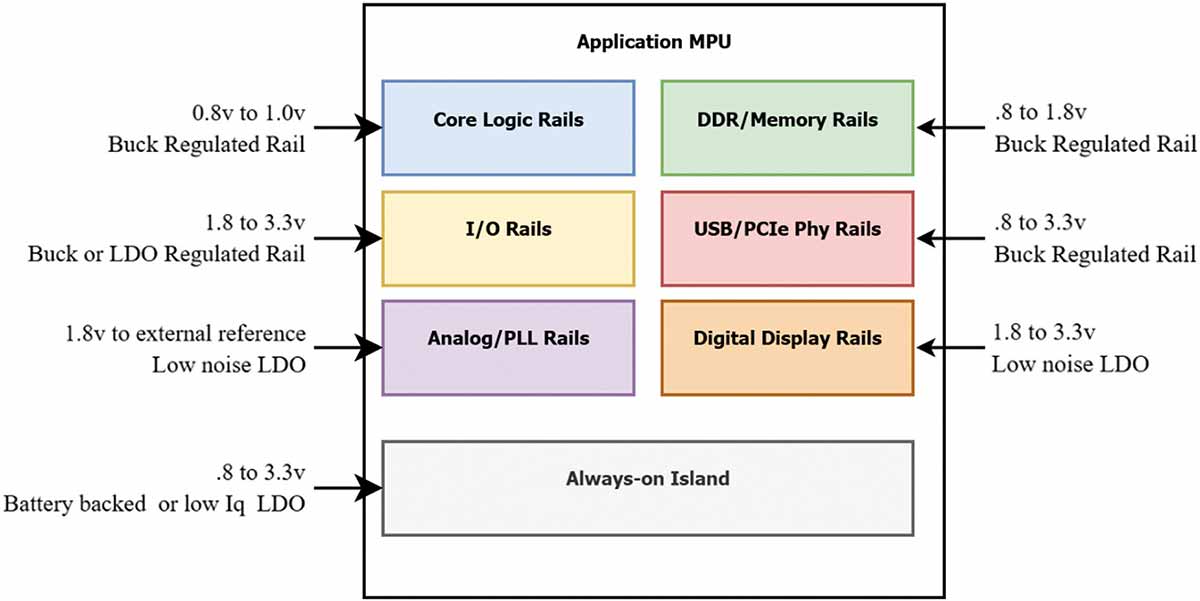
Memory Domain
I/O Domain
Each bank has its own V_IO pin, ordering requirements, and potentially its own voltage. Not attributing the right bank to the right V_IO rail is a source of failure when rail sequencing and level shifting.
Analog and PLL Domain
- In a PLL, in-band noise below a millivolt can still impact reference clock jitter. That can affect clock domains, such as a serializer/deserializer interface, and contribute to bit error rate issues.
- In-band noise in an ADC application raises integral non-linearity (INL) and reduces the effective number of bits (ENOB).
Always-On (AWO) Domain
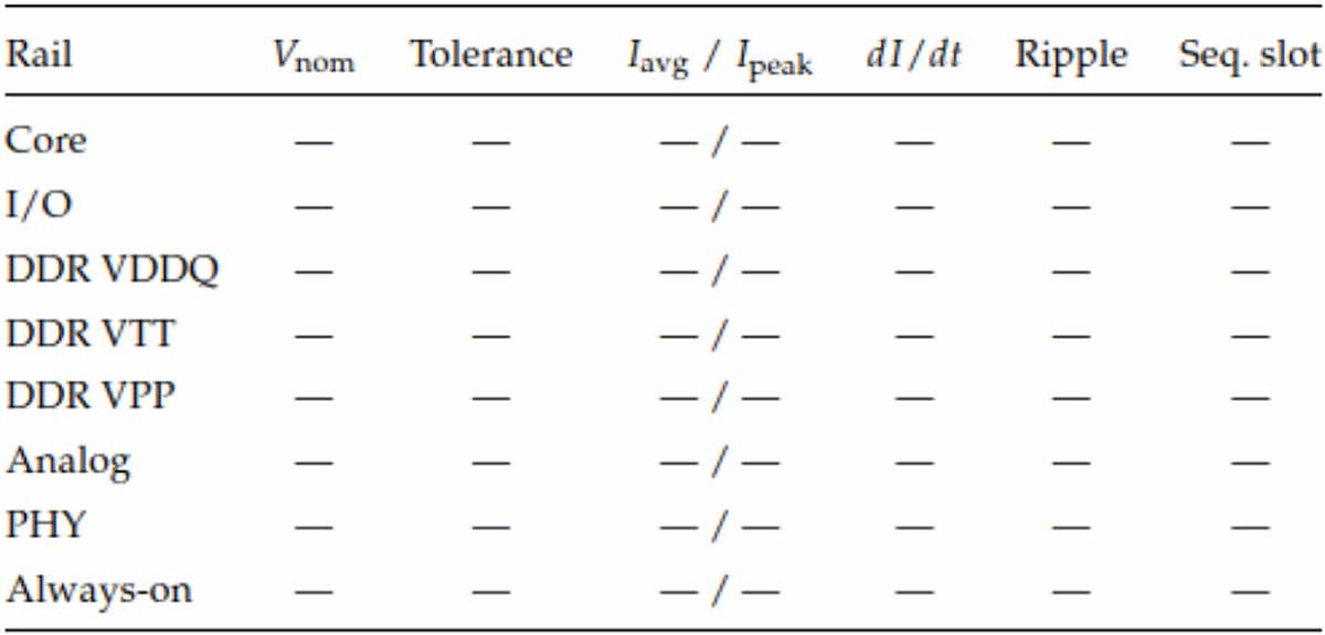
As a result, the first thing a hardware engineer should do when selecting a PMIC is tabularize the power domains. The table should pull out attributes such as nominal voltage, tolerance at the ball or pin, average and peak current in the operating mode of interest, load step (di/dt), in-band and out-of-band noise concerns, sequencing requirements, and standby leakage (see Table 1 for a suggested framework).
Average Current
Peak Current
Load Step
- They are difficult for the MPU silicon designer to estimate accurately, especially across all boundary conditions;
- They are difficult for the PMIC designer to support, because the control loop must respond quickly while remaining compensated enough to stay stable; and
- The MPU relies on local decoupling to prevent the core from dropping out during these switching conditions, while the PMIC must replenish the depleted decoupling capacitor.
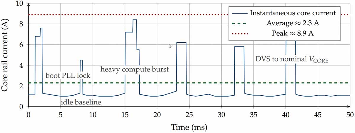
- When a datasheet defines a maximum-current table derived from different operating modes, which is conservative for most applications, the power supply designer should estimate the average current as 40% to 60% of that peak for an active workload.
- When a datasheet defines a quiescent-current specification on a per-domain basis, the power supply designer should look for leakage paths that could affect the current profile and confirm the operating conditions used for the measurement.
- IR-drop budgeting: For example, a 0.8 V core rail feeding a 6 A SoC/MPU across a PDN of 50 mΩ sees roughly 300 mV of DC drop, already beyond the processor tolerance window before any transient is considered. Local decoupling can carry the rail through transients, but remote sense at the load is mandatory in this case and drives routing concerns because the sense lines are noise-sensitive traces.
- PMIC accuracy versus rail accuracy: The regulator accuracy listed in the PMIC datasheet is not the same as the voltage tolerance at the processor ball. Sense routing, PDN drop, resistor tolerance, ripple, and transient droop all consume part of the rail budget.
- Explicit standby requirements: An always-on rail that draws 50 µA in deep sleep requires a PMIC whose enabled-channel quiescent current is comparable or smaller. A device that spends tens of microamps per enabled LDO will halve the standby battery life of a coin-cell-backed system regardless of the active-mode design. For PMICs with integrated coin-cell chargers or open-drain pins, the design must account for charger standby leakage, RTC quiescent draw, and the pullup paths used by the open-drain pins in the always-on budget.
To answer that question, the hardware designer has to account for what PMICs are known for: reduced area, reduced wiring complexity, centralized sequencing, and configurability. The tradeoff is vendor lock-in and less freedom inside each regulator channel.
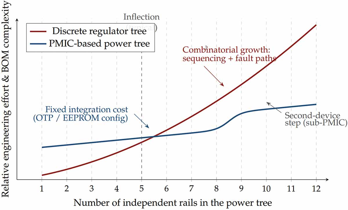
A PMIC works to flatten this curve by consolidating sequencing logic, power-good aggregation, and fault-response behavior into a single configurable block whose baseline correctness has been validated by the silicon vendor, rather than assembled from a chain of discrete power-good signals. The remaining integration work is system-focused and bounded: configuring the OTP or EEPROM, validating fault responses against the system needs, and laying out the device. Figure 3 illustrates the qualitative shape of the two curves and the inflection point where the PMIC becomes the lower-cost path.
- The system safety concept demands partitioning and the elimination of dependencies between devices that share the same die, package, or references;
- Field-repairable assemblies require the ability for returns to operate in a degraded state instead of the entire design failing to power up;
- A specific rail has noise-performance requirements that the PMIC cannot meet directly; or
- A single rail dominates the system power budget and requires an external-FET architecture for current or thermal reasons that an integrated-FET PMIC cannot match.
To better understand the unique nature of the blocks that make up a modern PMIC, we turn to the design choices that these devices force on the system.
This is where PMIC design differs from a collection of discrete regulators. With discrete supplies, the designer has more freedom to choose the controller, FETs, compensation network, switching frequency, current limit, and sometimes even the control architecture. In a PMIC, many of those choices are already embedded inside the device. The design task becomes less about creating each regulator and more about determining whether the PMIC’s fixed architecture matches the system’s electrical, thermal, sequencing, and noise requirements.
The switch resistance, RDS(on), is tied directly to the die area allotted to it. A larger switch reduces conduction loss and supports higher current, but it consumes more silicon area and increases package-level thermal stress. This is why many PMICs use fully integrated switching regulators for low- and mid-current rails, for example 6 A or less, while higher-current rails may move to an external-FET controller architecture. The exact point depends on voltage, package, thermal environment, and duty cycle, but integrated-switch solutions commonly become less attractive as currents move into the several-amp range.
The second limit is the set of parameters that defines how the regulator control loop functions. In a discrete regulator, the designer may choose the compensation components, inductor value, output capacitance, current limit, gate-drive strength, and loop bandwidth. In a PMIC, many of these are fixed or adjustable only over a narrow range. That simplifies design-in, at the cost of operating space. The external inductor and capacitor choices must remain inside the PMIC’s stability and transient-response assumptions. A rail that looks acceptable from a DC current perspective may still be a poor fit if the load transient, output-capacitance range, or startup behavior sits outside what the PMIC was designed to support.
In short, the system designer is betting that the PMIC validation team chose the right option set for the load. That is not always true, even when the same vendor provides the entire PMIC/MPU chipset.
The third limit is shared-resource behavior. A discrete regulator can often be evaluated as a mostly independent block. A PMIC regulator cannot. Its behavior is coupled to the other rails through shared silicon, package impedance, thermal paths, input supply paths, ground return, and control logic.
- The first category is shared physical resources. A high‑current buck may heat the die and reduce available thermal margin for nearby LDOs, references, or lower-current switching rails. Therefore, package temperature is not only a result of one rail’s load current. It is the combined result of all active rails, their duty cycles, their switching losses, and how heat moves through the package and board.
- The second category is shared electrical and control paths. A boost regulator may inject noise into a shared input, ground, or substrate path. A buck-boost rail may introduce higher RMS switch current and a less predictable noise profile than a simple step‑down rail. Startup timing, current-limit behavior, power‑good thresholds, and fault response may also be coordinated across multiple rails rather than contained within one regulator.
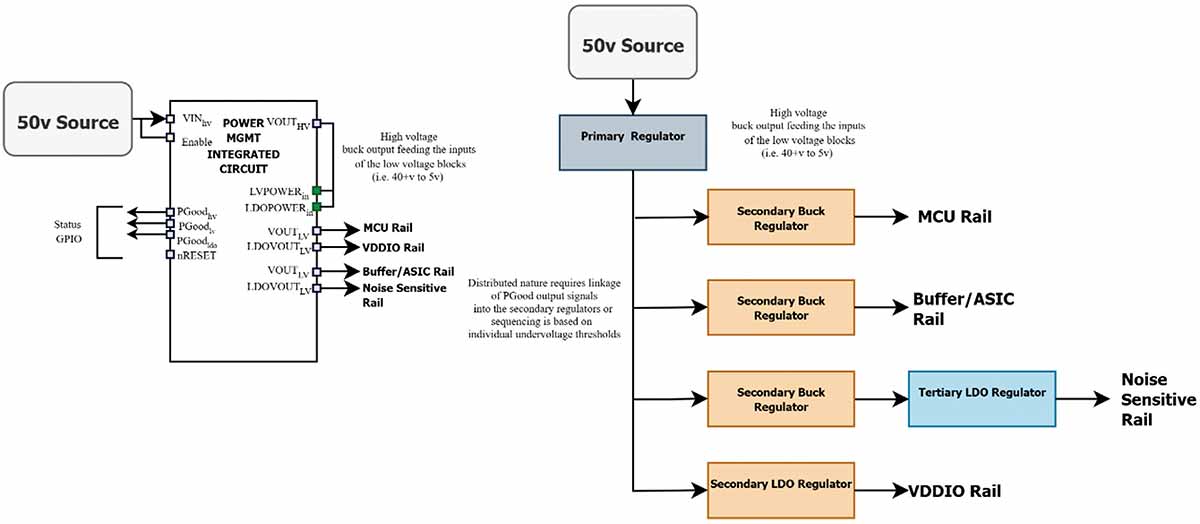
A common example is a 12 V to 24 V system being stepped down to 5.0 V or lower before feeding the downstream rails. This approach reduces voltage stress on the downstream regulators and improves integration density, but it also creates dependency. If the primary rail droops, current-limits, or enters a fault state, the downstream rails are affected. These high-voltage outputs are best abstracted as a cascaded power tree when analyzing efficiency and fault behavior.
Switching Type: Pulse Skipping vs. Forced PWM
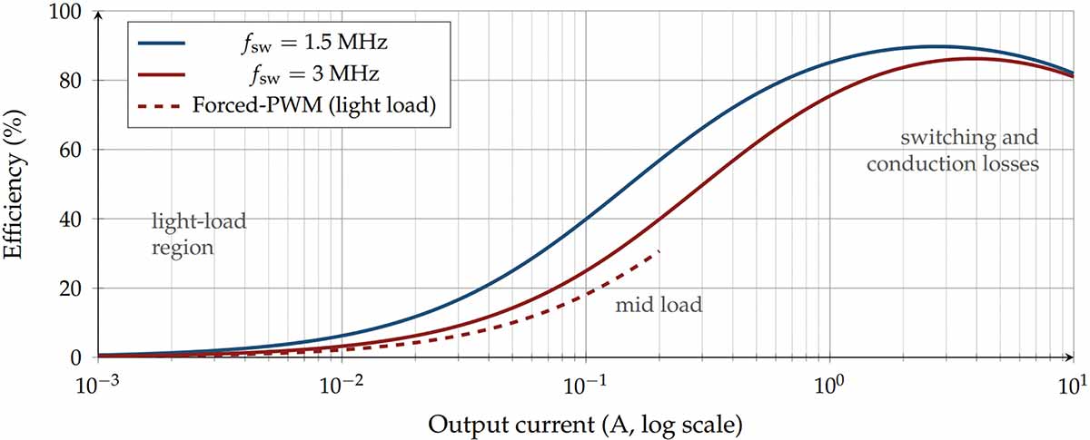
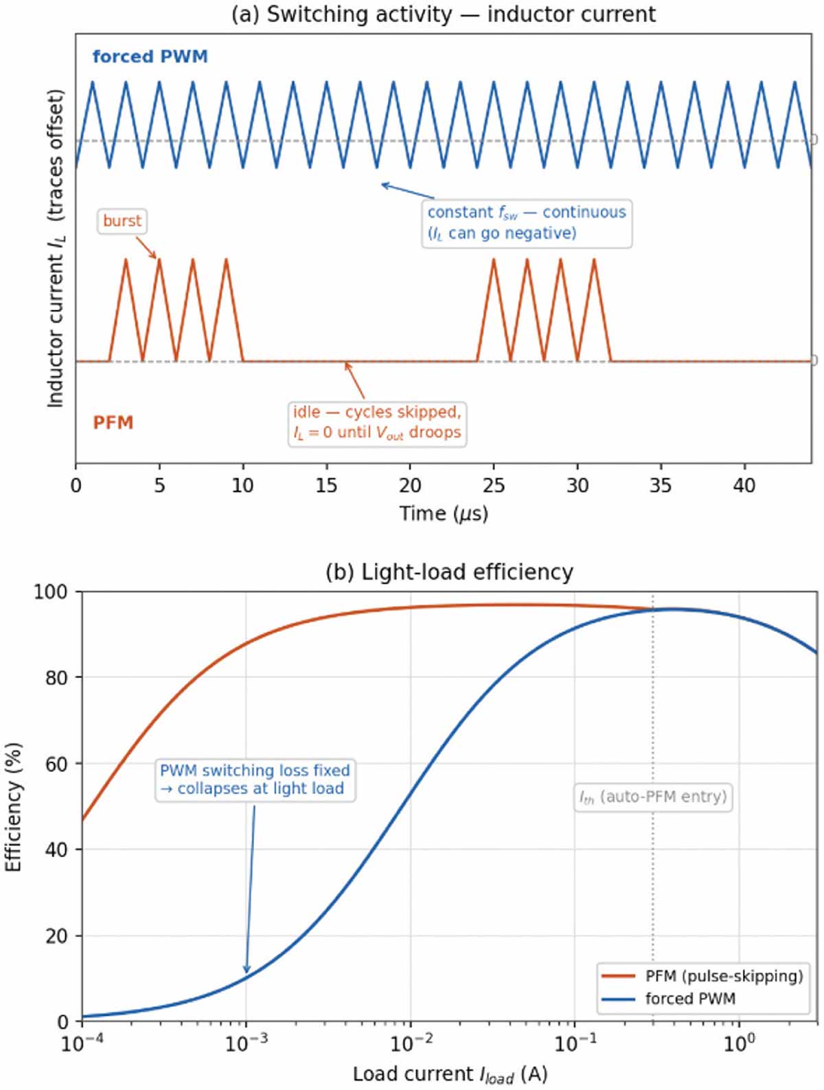
In forced-PWM mode, the regulator switches at a fixed frequency regardless of load. This makes the behavior predictable: the switching fundamental and associated harmonics stay in known locations. That predictability simplifies filtering, EMC planning, and coexistence with sensitive circuits such as RF receivers, ADCs, PLLs, clocks, and other low-noise analog functions. The penalty is light-load efficiency. At low current, switching losses and control overhead become a large fraction of the delivered output power, so a converter that is efficient at 2 A may perform poorly at 20 mA.
To improve light-load efficiency, many regulators offer pulse-skipping mode, also called PFM, skip mode, or burst mode, depending on the vendor. In this mode, the regulator reduces switching activity at light load. It delivers energy in bursts, then idles until the output voltage droops enough to require another switching event. This improves standby and sleep efficiency because switching loss falls with the effective switching rate.
The tradeoff is spectral behavior. The effective switching frequency now moves with load current, input voltage, output voltage, and the regulator’s skip-mode thresholds. A rail that is quiet in one state may produce low-frequency burst energy or shifting spurs in another.
Some system requirements need both modes. A rail may run in pulse-skipping mode during sleep, then switch to forced PWM before a radio event, ADC conversion, or other noise‑sensitive operating window. That decision belongs in the power requirements table, because the rail must account for timing, settling, and the load condition when the sensitive circuit becomes active.
There is also a spectral concern: if a PMIC automatically enters pulse-skipping below a load-current threshold, the worst EMI condition may occur when the system appears lightly loaded. For sensitive rails, the better default is often forced PWM unless the system has verified that skip-mode behavior is acceptable in every relevant operating state.
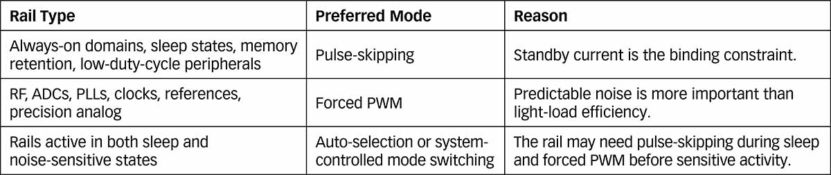
To make these mode choices easier to review, Table 2 provides a starting point.
Switching Frequency, Phase, and Spectrum Control
Unlike a discrete regulator, that heat is shared with the other rails, LDOs, references, protection circuits, and control logic inside the same device. A frequency choice that looks acceptable for one rail may reduce thermal margin for the full PMIC.
The next challenge is interaction between regulators. Several buck converters switching at unrelated frequencies can create conducted noise that moves through shared system resources such as return and power planes. Even if each rail meets its ripple requirement by itself, the combined switching behavior can create system-level noise that appears on clocks, ADC readings, or spectrum plots.
For both thermal and spectral reasons, PMIC switching behavior should be reviewed at the power-tree level, not rail by rail.
To address this, some PMICs allow rails to be synchronized, phase-shifted, or assigned related switching frequencies. This can reduce input-current peaks, spread thermal loading, and keep predictable spurs away from sensitive bands. It can also make the noise problem more deterministic, which is often preferable to several independent converters beating against each other.
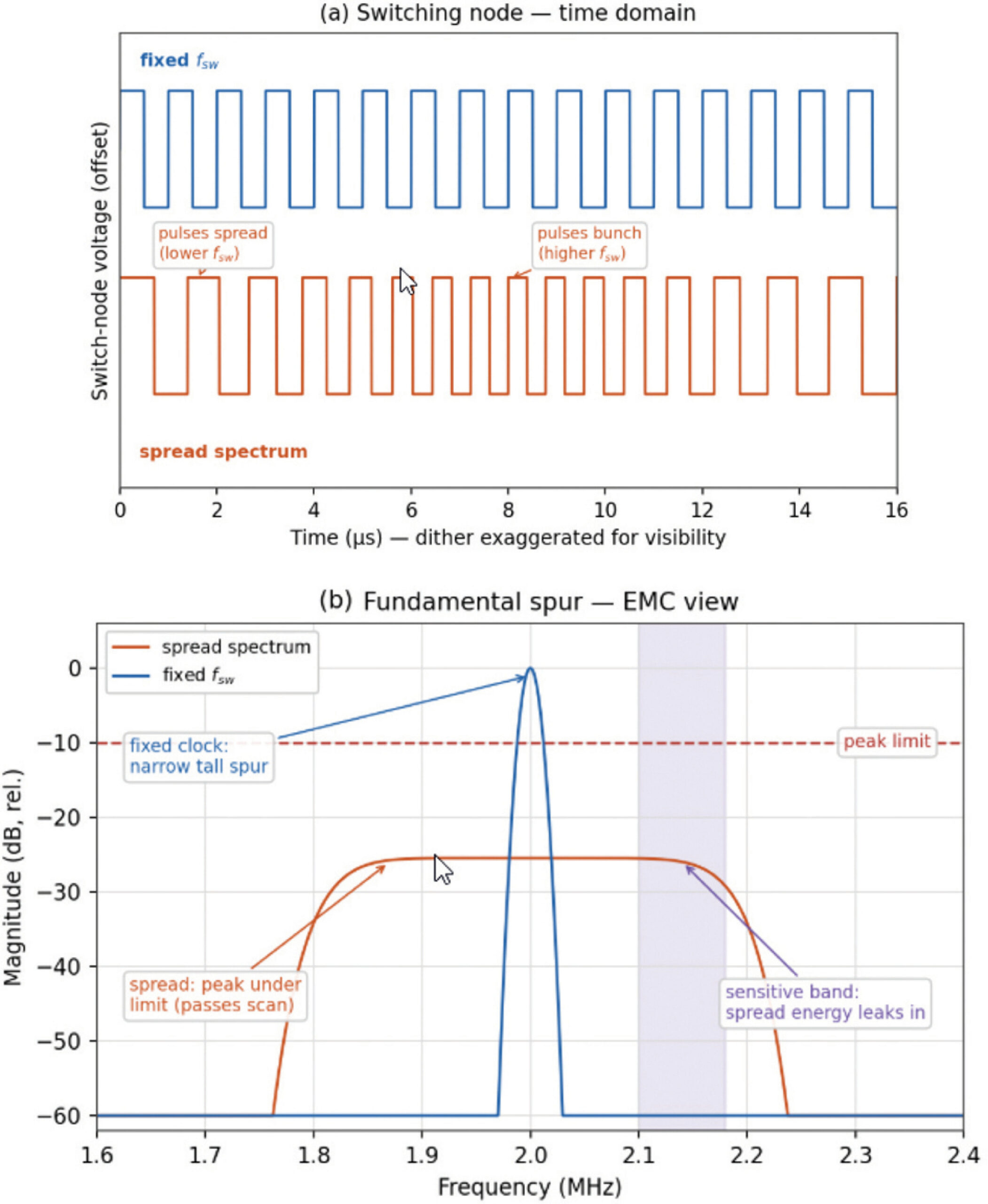
Another available control is spread-spectrum modulation, often enabled on one or more switching rails. Spread spectrum dithers the fundamental switching frequency over a defined range, reducing the peak height of narrow emissions spurs. This can help a product pass a peak-limited EMC scan, but it does not eliminate switching energy. It redistributes that energy across a wider band. That tradeoff matters when the PMIC sits near RF receivers, ADCs, PLLs, clock circuits, or precision sensors. A fixed spur can often be filtered, avoided, synchronized, or intentionally placed, but a spread-spectrum spur is harder to keep out of every sensitive band.
For PMIC selection, the important details are whether switching frequency is fixed or programmable, whether rails can be synchronized or phase-shifted, whether spread spectrum is enabled globally or per rail, and whether those settings remain valid across all power states.
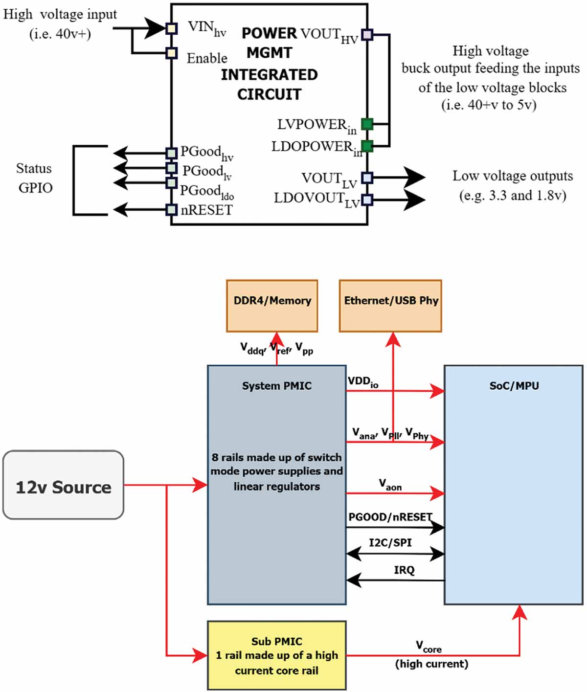
This means determining whether a regulator output is needed, mapping each rail to the correct PMIC output or external regulator, defining the power states, and then deciding which PMIC features the system actually needs. The PMIC forces the methodology away from a traditional rail-by-rail mindset and toward a system-level power-state-machine mindset, with digital logic controlling the transitions.
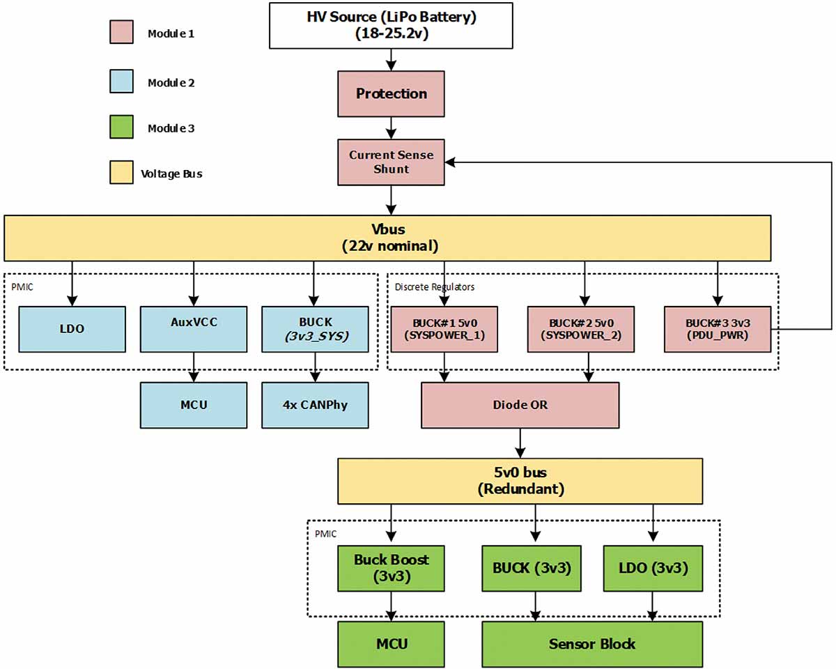
- The first item is the rail mapping itself. This is where the rail table developed in the previous sections is converted into a rail-to-rail architecture. Each PMIC output, LDO output, intermediate rail, and external regulator should be shown with the load or group of loads it supplies. The goal is to make it clear which regulator feeds each device domain, which rails are generated directly from the input supply, and which rails are generated from another intermediate supply.
- The second item is the control I/O. Enable pins, interrupt pins, reset pins, power-good signals, GPIO-controlled modes, and serial bus connections should be shown over the top of the power rails. This makes the signaling relationship visible before schematic capture. It also helps identify which signals must be valid before the host processor is running and which signals are only available after the firmware takes control.
- The third item is dependency. Sequencing dependencies, such as rail A before rail B, and fault dependencies, such as rail A collapsing and forcing rail B off, should be annotated directly on the diagram. The diagram should allow anyone reviewing the design to trace a rail back to the input source and forward to every downstream load without leaving the page.
A complete power tree makes these decisions visible rather than hiding them inside the schematic. Next, we focus on sequencing, including fault reactions and what to avoid.
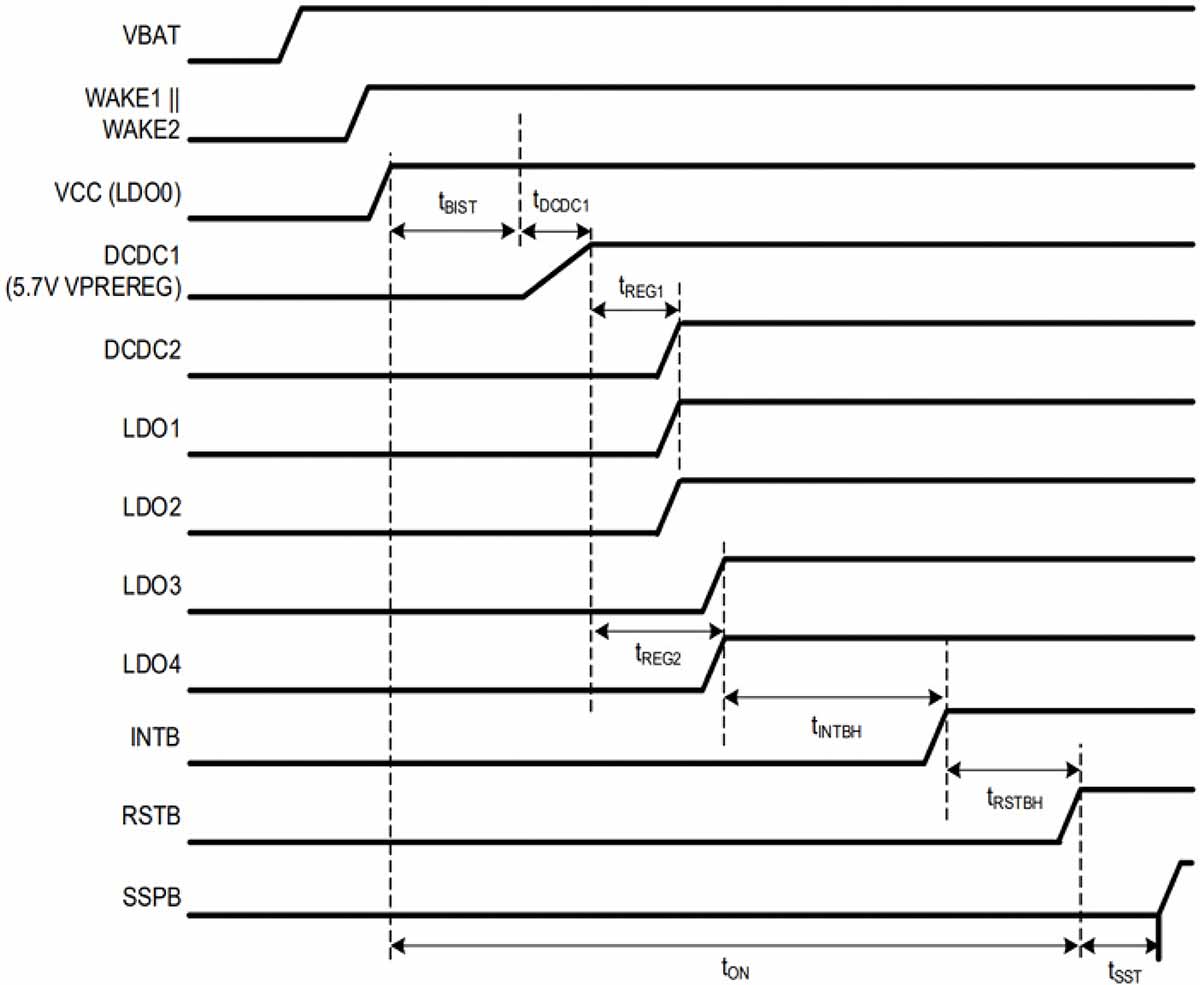
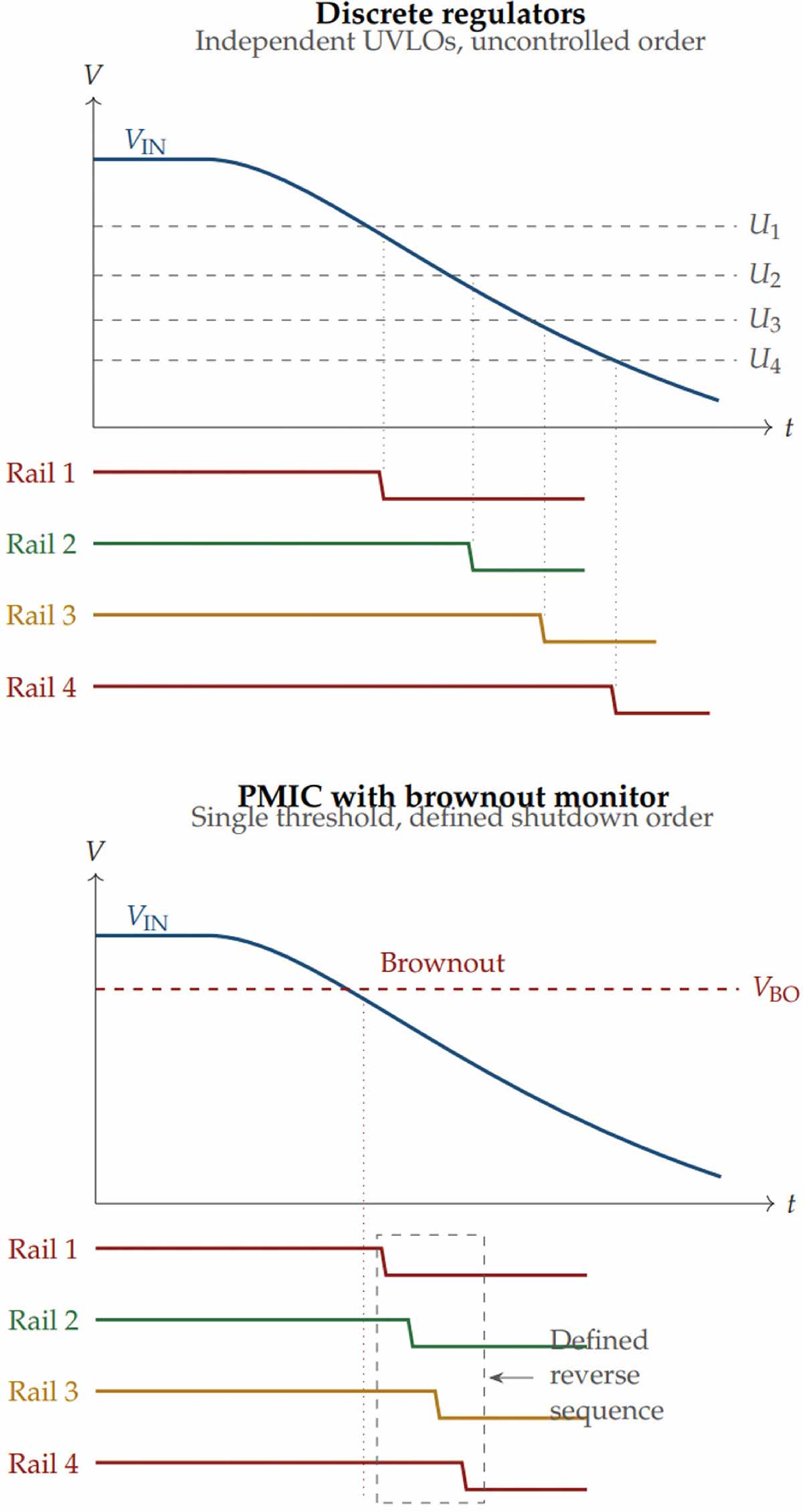
While the specifics of power-up and power‑down timing are tied to the needs of the individual system, special attention should be paid to power-down behavior under all circumstances. The PMIC does not eliminate undervoltage lockout (UVLO) or power-on reset (POR). Instead, it consolidates those functions into one device that can be detected by a single monitor and coordinated more easily. This allows a controlled shutdown of rails across all power domains in a defined reverse-sequencing order, while holding reset and power-good pins in defined states until the input rail fully decays.
Failing to protect against brownout or reverse sequencing can leave a core rail alive while the processor tries to execute code from a DDR controller that no longer has a valid voltage rail.
Contrast this with a legacy discrete architecture. An uncontrolled input brownout, such as in an inverter where motor voltages can keep the bus alive, can cause rails to fall at different times. This creates phantom failure modes that drift to the top of the debug list and are difficult to identify when the power-good pins are not tightly aligned to the system.
- What does the PMIC do after the fault is detected?
- How does it recover? and
- Who needs to know about it?
This naturally leads to fault recovery. PMICs generally implement two strategies:
- A latched fault preserves the failure condition and prevents repeated stress, but it may require a hardware reset, software command, or full power cycle to recover.
- Auto-retry or hiccup behavior improves field recovery, but it can also hide a marginal rail that repeatedly faults and restarts. This choice should be reviewed per rail, not only at the device level.
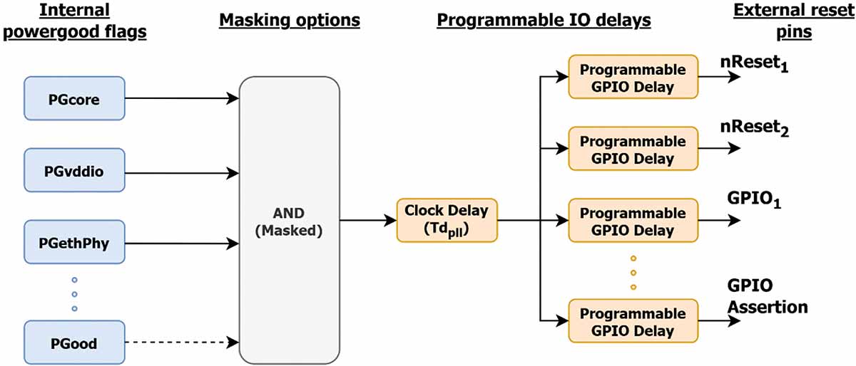
The designer should also understand whether fault bits latch until explicitly cleared, clear on read, or disappear after a reset or power cycle. Latching fault bits are useful for post-fault diagnosis, while clear-on-read behavior requires firmware discipline, so the first read is captured and logged before the evidence is lost.
Fault behavior should be documented in the same power-state table as sequencing. For each rail, define what fault conditions are monitored, what turns off, what stays alive, what is reported to the host, and what action is required for recovery.
- I2C is ubiquitous and low-cost, but slow;
- SPI is faster and physically more robust against bus hangs; and
- PMBus, which is rare in system PMICs but common in telecom and server point-of-load devices, standardizes the register map.
Configuration and storage are the second key decision. Most of these devices are simpler than modern controllers, and once one-time programmable memory (OTP) is burned, it is immutable. This is one of the most important characteristics driving PMIC design, because decisions made during the design phase lock the design into sequencing and reaction behavior that is usually evaluated late in validation.
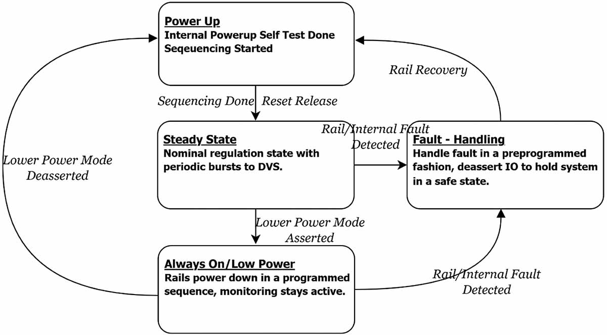
This produces a system design based on power states rather than voltage rails alone. A basic set of states that defines most systems is presented below:
- Power-up state: The focus is on the devices and rails that need to follow a specific power sequence. The failure modes to avoid are reverse biasing and improper signal gating before the system starts up and reset lines are released.
- Steady state: The focus, when necessary, shifts to high-power burst modes driven by functions such as dynamic voltage scaling (DVS), which may require firmware awareness.
- Fault-handling state: The fault handling and reaction strategy should be defined here. The questions are which failure modes require a fault-tolerant response, which require a fail-safe response, and how the system recovers.
- Always-on or low-power operating state: One or more states define how the device shuts down rails, enters pulse-skipping mode, and preserves retention behavior. Common failure points include leaving pins floating, which increases leakage current, and turning off rails required for retained memory.

Chris Semanson is a Senior Contributor to In Compliance Magazine, and is a Senior Staff Engineer in the systems and solutions team at Renesas Electronics. He has software and hardware experience across a wide range of applications in embedded systems, from automotive to inverter management at John Deere and Ford Motor Company.
Semanson holds a Master’s degree in Electrical Engineering from the University of Michigan Dearborn, where he studied under Mark Steffka in both computer and electrical engineering. He can be reached at chris.semanson@renesas.com