

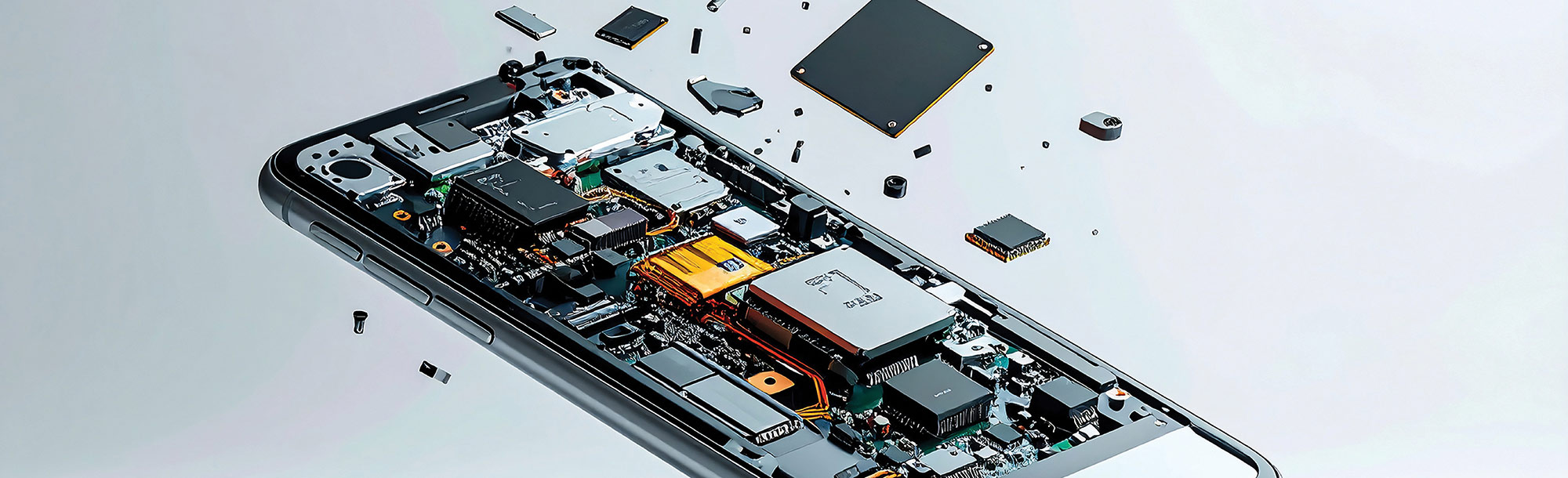
n recent years, the number of mounted semiconductor IC modules and the operating frequency have increased along with the enhancement of functions of smart phones. In the design of smart phones, the risk of electromagnetic interference (hereinafter referred to as EMI) generation is rising, leading to higher costs associated with EMC design.
Particularly, wireless receiver antennas are sensitive for unwanted electromagnetic radiation inside smart phones, posing a risk of radio frequency interference (hereinafter referred to as RFI), which can cause problems such as communication failures. One of the reasons for RFI is the noise radiated by semiconductor IC modules processing high-speed signals, located near wireless receiver antenna.1
Among the reasons, mobile industry processor interface (hereinafter referred to as MIPI) signals output by camera modules as image signals are prone to causing RFI. MIPI is one of the high-speed interface standards and transmits signals to motherboards via radiation-efficient flexible cables, thus causing relatively large noise radiation. Various studies have been conducted on analysis method2 and countermeasures3 for noise radiation caused by MIPI. Common countermeasures for noise radiation from MIPI signals propagated via flexible cables include conductive shielding and coating materials.4,5 These EMI countermeasure components are effective in suppressing noise radiation levels. However, these countermeasures require significant costs for component implementation and evaluation.
This paper proposes a low-cost system that automatically mitigates RFI in smart phones caused by noise radiated from flexible cables carrying MIPI signals. Figure 1 illustrates this concept. The application processor (hereinafter referred to as AP) calibrates the MIPI data rate through I2C communication with the image sensor, using received signal strength indicator (RSSI) within a channel as a feedback control variable, thereby mitigating the risk of RFI generation.
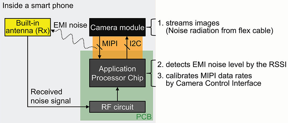
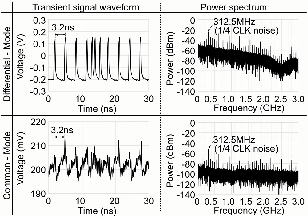
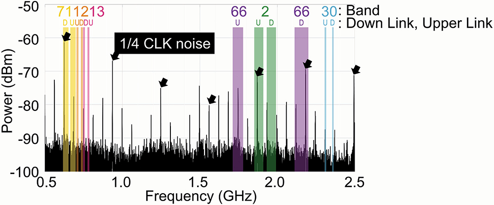
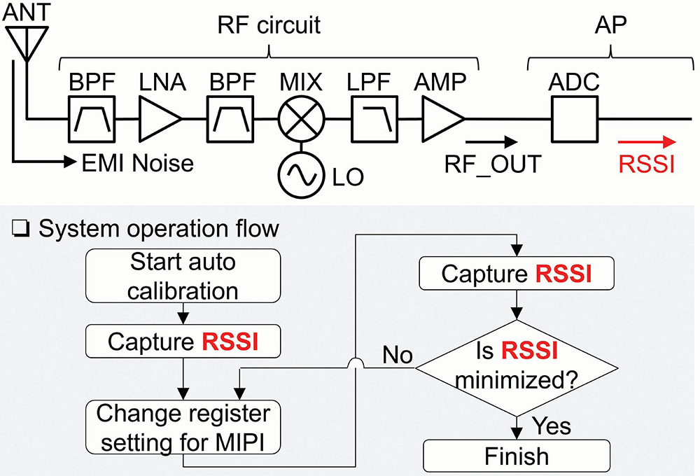
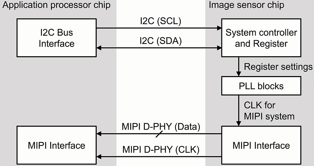
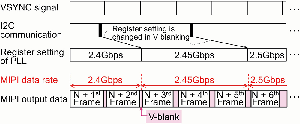
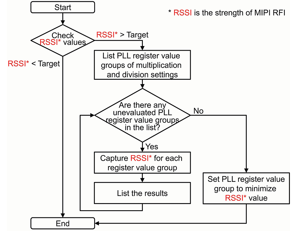
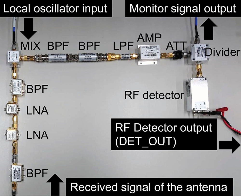
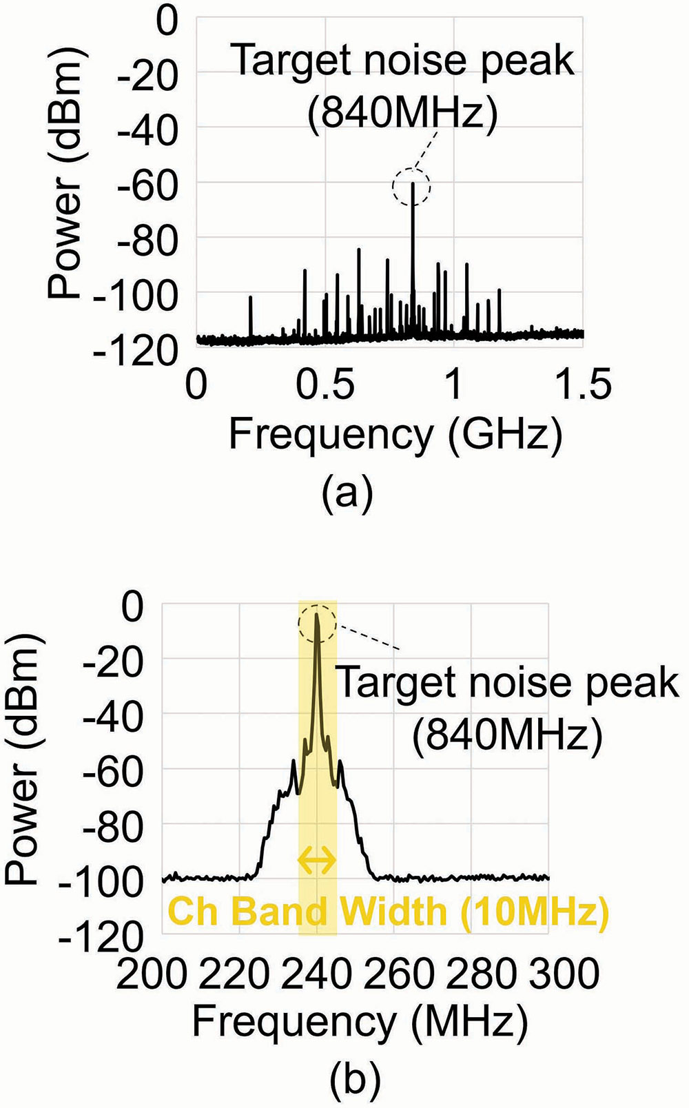
Figure 14 (b) shows the relationship between the MIPI D-PHY data rate and the RSSI detected by the RF detector. When the noise peak was at the center of the channel, the RSSI value was -3.2 dBm. On the other hand, applying our proposed system reduced the RSSI to -12.3 dBm, confirming the improvement of 9.1 dB. These results demonstrated the effectiveness of the proposed system in improving RSSI.
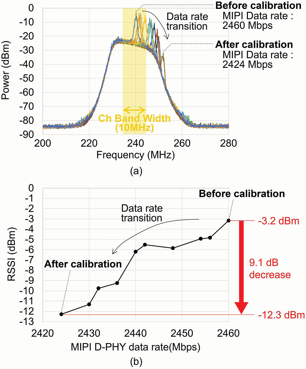
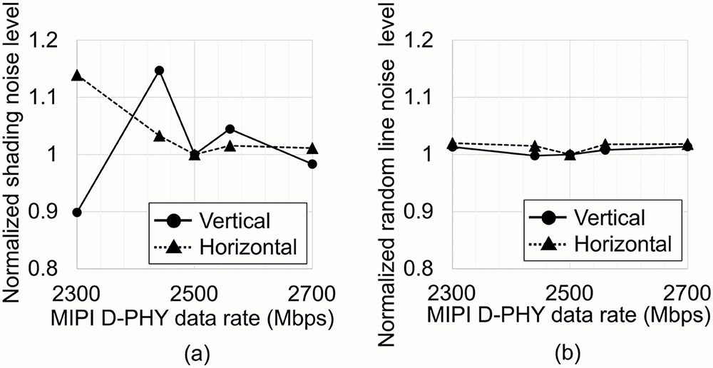
Figure 15 shows the results of measurements to check the relationship between the MIPI D-PHY data rate and image quality characteristics of the image sensor. The imaging condition was set too dark. The image quality characteristics are as follows: Dark shading is defined as the peak-to-peak values of the average signal levels of each vertical and horizontal pixel line. Random line noise is defined as the standard deviations of the signal levels of each vertical and horizontal line divided by square root of two. The values of each image quality characteristic are normalized based on the values at the data rate of 2496 Mbps.
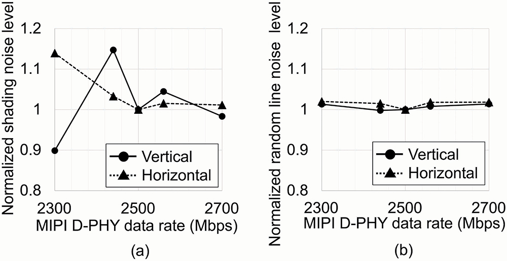
Figure 16 shows the measured probability that the proposed system could calibrate the MIPI D-PHY data rate when additive white Gaussian noise (hereinafter referred to as AWGN) was input to the RF circuit. AWGN, which is the thermal noise of a resistor amplified by an LNA, was input to the output terminal of the half-wave dipole antenna via a directional coupler. The increase in the power intensity of AWGN decreases the S/N ratio. Under these conditions, the reduction in RSSI when the noise peak of the MIPI D-PHY moves out of the channel becomes smaller, and calibrating the data rate of the MIPI D-PHY becomes difficult for an AP. In calculating the S/N ratio, a signal power was defined as the maximum power of a single peak of the MIPI D-PHY mixed into the center of the channel. On the other hand, a noise power was defined as the maximum total power of AWGN existing in the channel. The number of attempts to search for the optimal MIPI D-PHY data rate by the proposed system was set to 20. The measurements confirmed that 0 dB or higher S/N ratio allows the proposed system to calibrate the MIPI D-PHY data rate with 100% probability.
- S. Kim et al., “Simulation-based analysis on EMI effect in LPDDR interface for mitigating RFI in a mobile environment,” 2016 IEEE 20th Workshop on Signal and Power Integrity (SPI), 2016, pp. 1-4.
- Y. Han, S. Lee, H. A. Huynh, and S. Kim, “Radio Frequency Interference Analysis of Camera Module and Antenna in Smartphones,” 2019 International Conference on Electronics, Information, and Communication (ICEIC), 2019, pp. 512-515.
- Y. Chien, H. Liu, C. Chou, and T. Wu, “An Embedded Common-Mode Filter and Mixed-Mode Scattering Parameters for the MIPI C-PHY Interface,” IEEE Transactions on Electromagnetic Compatibility, vol. 66, no. 1, pp. 143-152, Feb. 2024.
- R. Kumar, A. Kumar, and D. Kumar, “RFI/EMI/microwave shielding behaviour of metallized fabric-a theoretical approach,” International Conference on Electromagnetic Interference and Compatibility ‘99 (IEEE Cat. No. 99TH 8487), 1997, pp. 447-450.
- S. Yang et al., “Effects of Shielding Materials on EMI Performance for 5G Wi-Fi Applications,” 2022 17th International Microsystems, Packaging, Assembly and Circuits Technology Conference (IMPACT), 2022, pp. 9-12.
- MIPI alliance specification for D-PHY version 3.0, July 2021.
- “3GPP TS 36.101: User Equipment (UE) Radio Transmission and Reception (Release 12),” September 2024.

Akihiro Tsukioka is part of the Design Platform Technology Division at Sony Semiconductor Solutions Corporation and can be reached at akihiro.tsukioka@sony.com.

yasuhiro.ochiai@sony.com.