
ssues related to electromagnetic compatibility (EMC) are often identified during qualification testing in an accredited EMC test lab which typically occurs late in the product design cycle. Obtaining a cost-effective solution to these EMC issues may be time-consuming, and many EMC labs can be fully booked or have limited availability, have long lead times, or involve significant costs. But inexpensive test equipment and procedures (let’s call them thrifty methods) used for helping to solve these EMC issues outside an EMC lab are very desirable, especially if no in-house EMC facilities are readily available.
There are several excellent resources for troubleshooting methods and building a low-cost EMC toolkit.1 This article offers some other test equipment options that have different capabilities and which can be even less costly. Although the thrifty method is mainly used to compare results before and after implementing a fix (not meeting a specification limit), with some experience, it can also be used in the pre-qualification development stage early in the design cycle to identify potential issues before formal lab testing. Identifying issues early allows maximum flexibility to experiment and provides sufficient time to make cost-effective changes before a design is frozen and difficult to change.
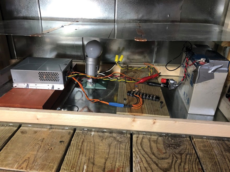
To evaluate radiated emissions, I’ve used a variation of a TEM cell (see Figure 6a-c) for over a decade. Such an enclosure is required to keep out ambient radiation such as AM/FM radio. Although you cannot compare results on an absolute level as those obtainable in an EMC lab anechoic chamber, the use of a TEM cell shows similar trends. For example, if the improvement for a particular fix is x dB, there will be similar improvement in an EMC lab chamber.
This homemade cell is made from HVAC sheet metal ducting available at many home improvement stores. The dimensions are 16 x 16 x 37 inches, with a center plate (without end tapers) of 32 x 13.5 inches. The center plate height is adjustable to accommodate different DUT sizes (default is in center between top and bottom). Figure 6b shows a small opening in the door. This opening is to help isolate the source of the noise (DUT, harness, or both) by allowing placement of the harness outside the TEM cell.
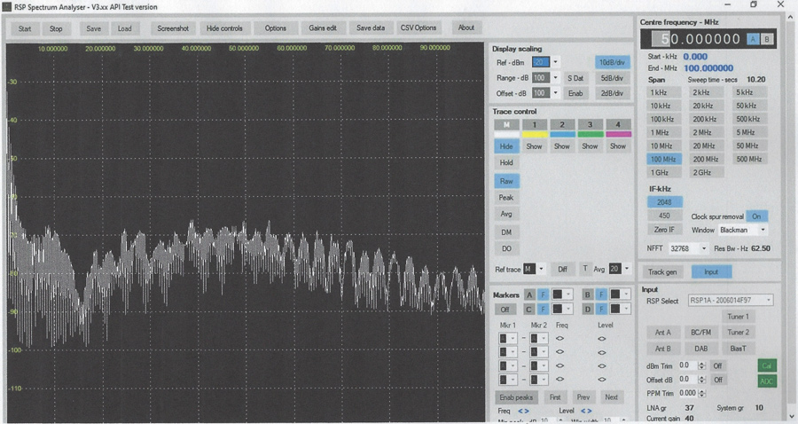
In Figure 6d, looking at the S11 and voltage standing wave ratio (VSWR), it appears that this TEM cell is only useful for frequencies less than about 200 MHz. However, it has been used with success in finding fixes for frequencies greater than 1 GHz. Since we are only using the TEM cell to assess “before and after” results from any fixes, any discrepancies can usually be ignored as long as the DUT and harness locations are controlled (i.e., consistency in DUT positioning and orientation). In an anechoic chamber, the antenna is much farther from the DUT and harness than in this homemade chamber, and proximity coupling with DUT variation is less of an issue.
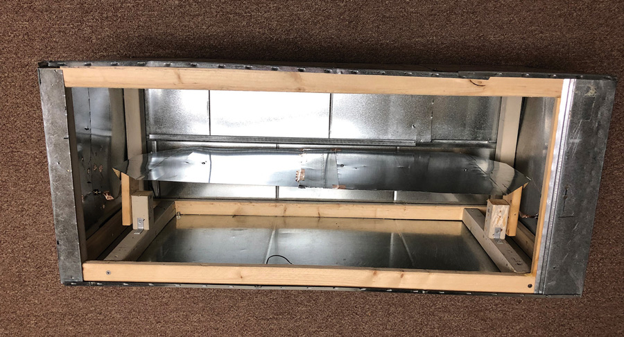
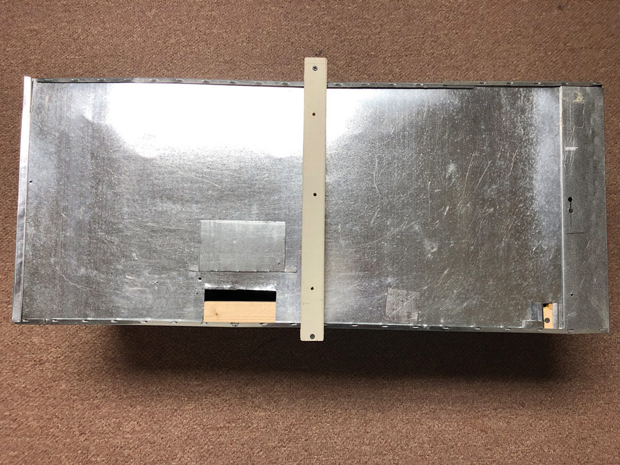
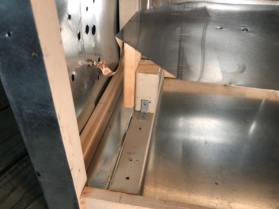
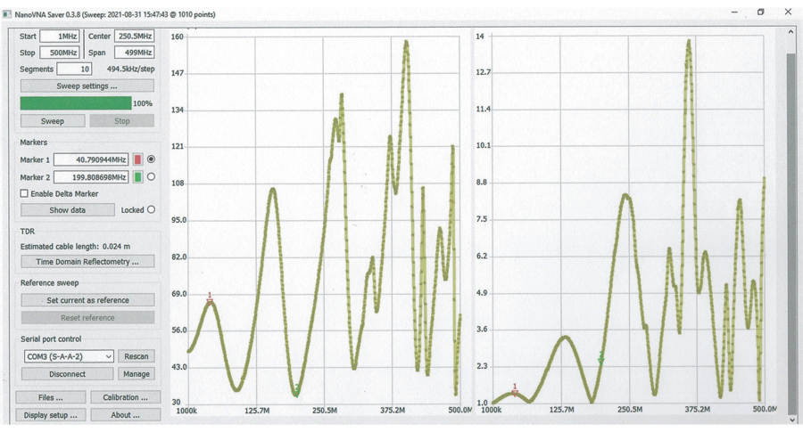
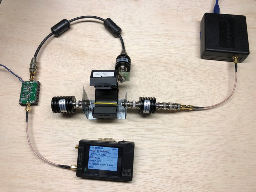
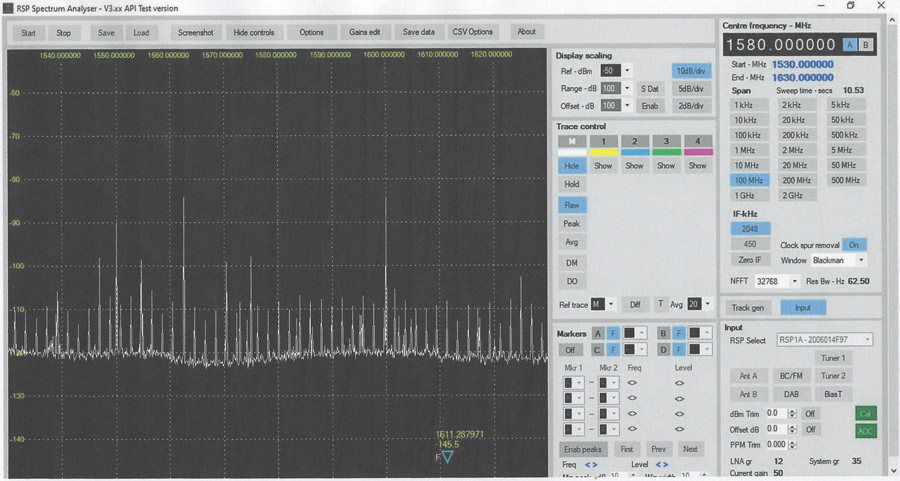
Figure 7d shows a calibration setup using a signal generator feeding an RF power amp whose output feeds a 3 dB attenuator and the BCI probe. The induced current is measured with a cheap version of the BCI calibration jig. The voltage is measured across a 50-ohm, 10 dB attenuator leading to the spectrum analyzer. Induced current was measured at over 2 – 350 MHz, and the maximum is about 100 mA rms which is similar to what is required to meet most automotive EMC specifications.


The next potential culprit was thought to be due to ESD. Testing as shown in Figure 11 (PCB over ground plane) showed that this was indeed the root cause problem. The ESD gun was applied directly to each pin of the suspect IC (air discharge not repeatable). The IC had one pin that had much lower immunity (< 2 kV, one discharge) than the other pins (> 6 kV, multiple discharges). To determine this immunity, many PCBs were sacrificed.

- See, for example, EMI Troubleshooting Cookbook for Product Designers by Patrick G. Andre and Kenneth Wyatt.
- Detailed information about the NanoVNA is available at https://nanorfe.com.
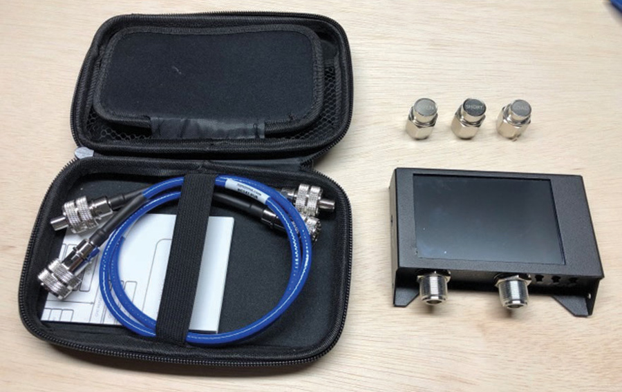
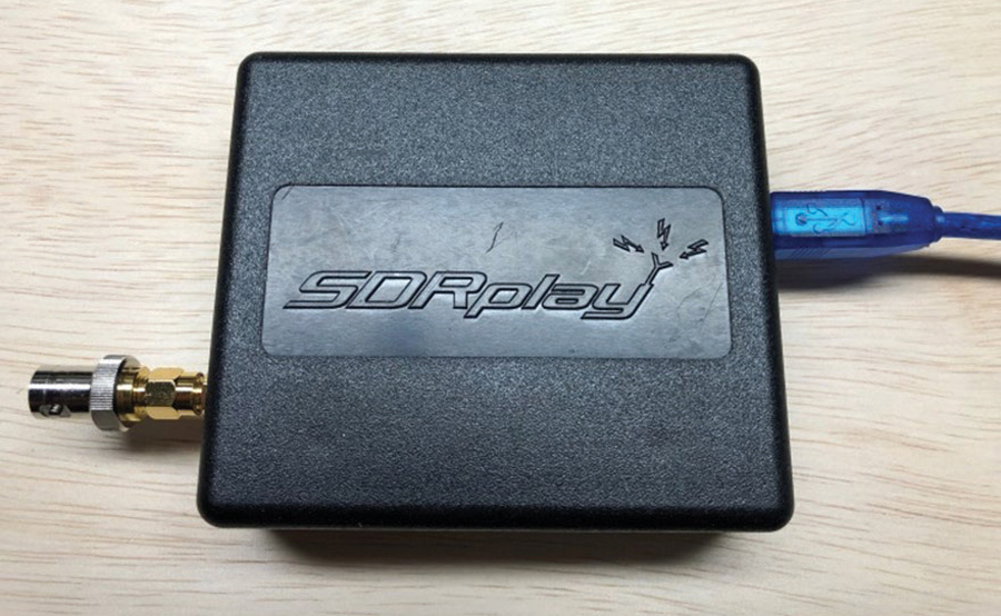
- Detailed information about the SDRplay is available at https://www.sdrplay.com.
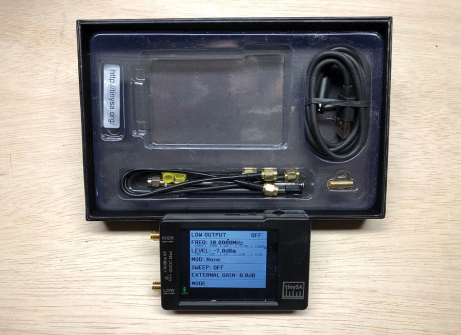
- Detailed information about the TinySA is available at https://www.tinysa.org/wiki.
- See “Injection Probe Modeling for Bulk Current Injection Test on Multi Conductor Transmission Lines” by Frédéric Lafon, Younes Benlakhouy, and François de Daran for a cut-away of the BCI probe shown in Figure 7a.
- SAE J2628, Characterization, Conducted Immunity.
- For a detailed comparison of these transients and ISO 7637-2, see “Comparison of ISO 7637 Transient Waveforms to Real World Automotive Transient Phenomena” by Keith Frazier and Sheran Alles, 2005 IEEE EMC Symposium.
