ang around embedded software engineers long enough and the words design for test or test-driven development will become commonplace. This is because in a world where functionality is ever-increasing in complexity, you need to be able to both verify and validate your device’s functionality such that it matches the requirements. And, while these design practices are well understood in digital systems made up of microcontrollers (MCUs) or system-on-chip devices (SoC) with functional safety driving extremely distributed systems, they are just as applicable in low level mixed-signal devices.
Gone are the days where the main MCU of the embedded module is trusted to do everything; in industrial and automotive systems where safety is critical, there now exist other devices to help test the main microcontroller to aid in the safety integrity level (SIL) of the device. These functions vary in complexity and range from helping the MCU toggle pins to ensure stuck at faults are mitigated, to helping verify complex question and answer watchdog issues, and voltage monitoring functionality.
Often the next smartest device in the system is either another low-level MCU or, in the quest to simplify a bill of material (BOM), a power management device (a PMIC) with dedicated safety functions. And since these devices don’t have flash memory and are traditionally analog in nature, it makes the validation of these devices somewhat challenging for engineers who traditionally focus mostly on transient load responses.
To aid in helping an engineer develop a test philosophy for such a device, we will focus on a distributed system made up of both MCU and PMIC. The article will use this system to demonstrate validation concepts that system designers have been employing for quite some time, the simplest of which is an open loop test philosophy and its strengths and weaknesses. The closed or in-the-loop based test philosophy will address those weaknesses and demonstrate how one can easily expand upon their test setup by including an MCU to model the system or system device. Taking these two test philosophies together will shed light on how exactly a design-for-test philosophy can be adopted for a traditional analog-based device such as a PMIC.
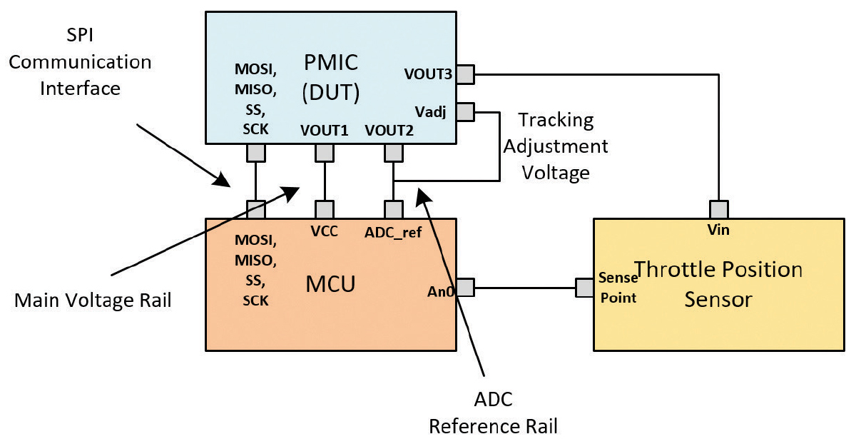
This system is outlined in Figure 2, made up of a high-end MCU, a power management device, along with an external sensor that will monitor throttle position.

Each active device in this example, the MCU and PMIC, needs to go through two types of testing prior to starting their task. The requisite testing includes:
- Internal self-testing – each device undergoes a self-diagnosis to ensure proper operation (typically resulting in an external pin being toggled to let other devices know the state of these tests). This type of test is usually defined as a built-in self-test (BIST).
- External system requirements – a wide variety of systems tests requiring different devices to properly diagnose interfaces and different peripherals of the microcontroller. These tests are more complex, typically requiring a communications interface between devices which allow the devices to signal when and how a test is to occur.
In summary, our example system functionality includes requirements such as the ability to:
- Verify pins at startup to ensure critical low voltage pins are not shorted;
- Verify analog to digital converter (ADC) functionality; and
- Verify that the serial interface and internal registers are working properly.
- Verify pins at startup to ensure critical low voltage pins are not shorted;
- Verify analog to digital converter (ADC) functionality; and
- Verify that the serial interface and internal registers are working properly.
When it comes to testing these embedded functions, the focus must be on developing a test setup that allows the PMIC team to ensure that these functions work properly by exercising their pass-fail criteria. Because of the variety of functionality to test, validation can be done in one of the following two ways with low-cost devices that are easy to implement and program:
- Open loop testing, in which the device is commanded to perform a required action and the device demonstrates the acceptance or failure of that test. This is often done without a ‘plant’ in the system.
- Closed, or in-the-loop, testing, in which the device is commanded to perform an action, such as toggle a pin, and a receiving device confirms the action. This is often done with a plant, acting as a model of the system.

- Input/output pin level, or
- A serial communications interface, such as a I2C or serial peripheral interface (SPI).
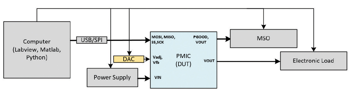
Overall, the goal of an open loop setup is to be able to communicate not only to the device under test (DUT, in this case, the PMIC) but to trigger measurement devices to automate as much of the test sequencing as possible. An example setup is found in Figure 4.

In order to demonstrate how to evaluate the effectiveness of our open loop test setup and its ability to interface, we’ll examine two system test cases denoted by our example system; they are:
- Test Case 1: A fault reaction and accuracy test, where the DUT is cycled through internal codes which correspond to a limit read by the ADC, and the fault reaction is measured via a GPIO pin.
- Test Case 2: An external reset command that allows an external device to trigger an internal function inside of the PMIC. In this case, we’re validating to ensure that at least one of the three PMIC rails can be reset via SPI.
- An SPI addressable digital to analog controller (DAC).
- A triggerable mixed signal oscilloscope (MSO)
- A USB to SPI converter
- An addressable power supply
- A programmable load
- Set the MSO to send a specific SPI message to the DAC.
- At the same time, sweeping the VIN voltage with the power supply, and
- Later, command the load to move in and out of the allowable range as you sweep the DAC voltage.
- An MSO capable of triggering off an SPI message from the computer to the DUT, and
- A USB to SPI converter.
The setup is found in Figure 6.

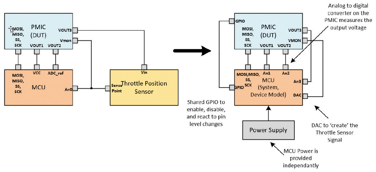
However, where this setup falls short is in the modeling of an actual embedded system. The assessed functionality is limited to just the DUT and the actions of the DUT in response to directed stimuli and does not include the interaction of the DUT with the accompanying MCU in response to those stimuli. For that, we turn to a closed loop setup or a system model.
- How does the control loop function in the presence of a load step? Or,
- How does the controller function with a varying input voltage?
Both of these examples employ a simple oscilloscope and power supply, with an engineer performing a manual evaluation of the setup. However, in a mixed signal design that is highly integrated with a microcontroller, this approach is limited. To address this, we turn to a model of the system with the MCU in it. There is a wide variety of ways to accomplish this, including:
- Model in the loop (MIL) or software in the loop (SIL), in which a software model of the system is made and exercised based on requirements;
- Processor, or MCU in the loop (PIL), in which a processor is used to create stimulus and measure reactions, based on the requirements to the system; or
- Hardware in the loop (HIL), in which the actual target hardware used is similar to that of the end system.
An MCU offers the example test system a lot of freedom in how to evaluate. Among the many advantages are:
- It can offer breakpoints in the code execution, meaning that you can look for complex interactions and break when the MCU encounters them. These can come in the form of common hardware breakpoints or test assertions.
- It has built-in peripherals such as high-speed timers, DACs, analog to digital converters, and a wide variety of communications interfaces to help exercise the DUT.
- It offers memory that allows the device to sit and buffer results and store them or print them to a UART for easy data logging.
- It is largely independent of user interaction, meaning that once programmed, it can run without being monitored for long periods of time and sometimes even indefinitely.
In our example throttle-by-wire system, the addition of the microcontroller allows us to introduce more complex test scenarios. Two examples of these more complex scenarios are:
- Like our open loop fault reaction test, we can now interact with the microcontroller and test fault reaction and recovery of the PMIC/MCU system to an externally triggered fault, while varying the input voltage to the system.
- We can also test the interaction between the MCU’s internal watchdog and the PMIC’s ability to reset the MCU in the case of a watchdog error.
- How the MCU/PMIC interaction controls execution order (here we introduce a concept called state driven testing); and
- How the MCU/PMIC interaction can implement modularity in terms of testing modularity such that we’re able to take different execution paths in the same function. This specifically addresses requirements of ensuring that a mechanism or function demonstrates pass-fail functionality.
Taking these into account, we’ll now discuss some embedded C-level constructs that can be used in order to control execution and to address our modularity requirement. Together, these will give us a great amount of flexibility in debugging and regression testing.
An example, depicted in Figure 8, is a state diagram that outlines the startup and initialization tests between the two devices in our example system, the PMIC and the MCU.

This design pattern is borrowed from a universal verification methodology (UVM). With this context, we can define a finite state machine as a computational model used to simulate sequential logic in a ‘stateful’ means. It allows abstraction of a complex series of events to a series of states to control execution flow.
The implementation is usually done in C and follows a design pattern similar to that in Figure 8. An example of its instantiation is shown in Figure 9.
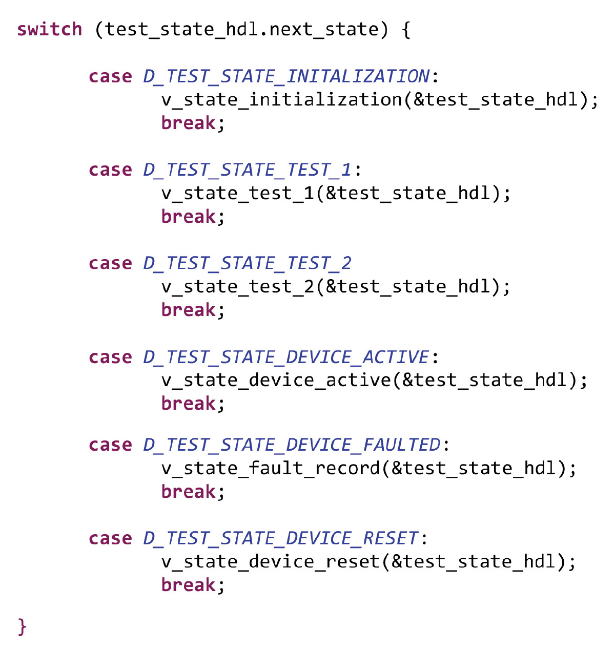
For example, for the system to move from the initialization state to a communications interface state, the combination has to match the expected behavior. If it does, this successfully satisfies the pass case. Otherwise, the test would signify a failure and the fail case would be able to be validated.
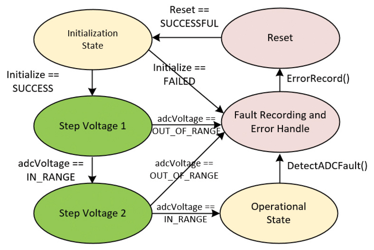
Another example, shown in Figure 10, demonstrates how the state machine can control the order of execution to a finite end.

By implementing this concept as a state machine, depicted in Figure 11, the system can easily validate both the pass case, in which the system recovers, as well as the fail case in which the system goes to an error state.
In production environments, build options (sometimes referred to as compile switches) are a powerful tool to create modularity in firmware for building various embedded targets or multiple applications. Inside a disciplined organization, multiple people using the same compile switch can reconfigure an entire application by compiling large sections of data in and out instead of creating, tracking, and supporting new firmware variants.
However, in a state driven test environment, the goal is not to be memory efficient but to be able to support a wide variety of test cases in a single design pattern to take advantage of the software architecture choice. To demonstrate how powerful these test cases can be, we present two test cases in which our embedded system model needs to perform a test of:
- The watchdog (WDT), including both a simple window watchdog function and a challenge-response watchdog; and
- An external pin toggle, in which the MCU commands the PMIC to toggle a GPIO and the MCU would be forced to acknowledge it.

In the case of the external pin, we simply create three functions:
- We toggle the pin high, then low, and observe the expected response.
- We do not toggle the pin at all, simulating a pin stuck fault due to a solder short, and observe the expected response.
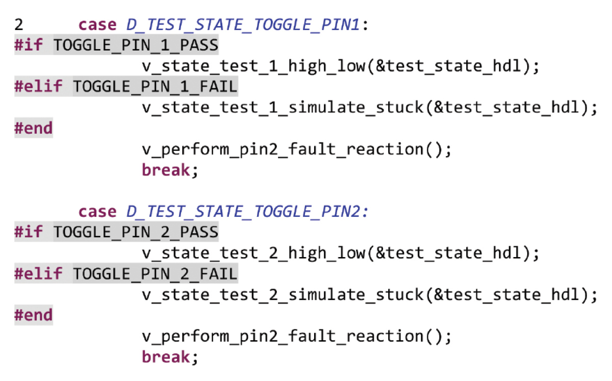
However, this C construct is not without risk. The main dangers of overuse of these build switches is their complexity and the ability to document them, especially when they appear in various sections throughout the validation application. Overuse and poor discipline can create a complex set of decisions that are difficult to maintain, let alone pass to another validation engineer. To combat these, we suggest to:
- Refactor the code often as new test cases and functionality are created, with a focus on making each function and test atomic so each compile switch is localized.
- Document the flow of the test as you develop your validation firmware. Something as simple as a test flow chart, for example, can be invaluable when ensuring the firmware is designed properly.
By implementing a state driven test concept in a closed loop system with a model of the target embedded device, you can achieve higher validation coverage and create a method to help identify and fix those hard-to-catch bugs before release!