hen helping clients in the electric vehicle (EV) industry with their module design, I often find that engineers tend to follow an out-of-date list of “do’s” and “don’ts” in the form of EMC design rules without understanding the basics. These kinds of design rules are often borrowed from other industries, and they are not up to date with the latest technology involved in the fast-paced EV industry.
In this article, using a powertrain module as an example, I will first introduce the high voltage EMC regulations with which a powertrain module needs to comply. I will then highlight the risks and challenges when designing such modules. The main part of this article will share design techniques that engineers can apply on various parts of a powertrain module, including ground, front-end filter, inverter design, and so on. Examples are given to demonstrate some of the key design techniques.
It should be noted that the introduced design techniques in this article share the same principles as any other EMC engineering. Therefore, engineers from other industries can also benefit from these techniques.
Powertrain modules are one of the key differentiators in the EV industry. Both vehicle manufacturers and Tier-1 suppliers have been spending considerable resources researching and developing state-of-the-art technologies for EVs. The current trend is to achieve a more compact module design with higher power density and system efficiency. For instance, the Nissan LEAF has achieved a very compact e-powertrain module design by integrating an on-board charger (OBC), a DC-DC converter, and a junction box with the electric drive unit (EDU) [2].
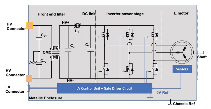
This article presents the EMC design of a powertrain module, which consists of an electric motor, an inverter, and a mechanical gearbox. The electric system diagram of an EV powertrain module is illustrated in Figure 1.
The importance of design engineers taking a system-level overview of an EV powertrain module was presented in my previous work, “Demystifying EMC in an Electric Vehicle’s Drive Unit” [3]. It is critical to factor in EMC design considerations at an early stage so as to achieve the overall system design goal. The high voltage (HV) EMC regulations and requirements present a daunting task for not only new entrants but also for well-established companies in the automotive industry. Therefore, we’ll first review in this article the HV standards and regulations that apply to electric powertrain modules. Then, we’ll highlight EMC challenges in the powertrain module design and demonstrate design techniques to address potential EMC issues. Engineers will then have a better understanding of how to design a module that will pass the EMC requirements in the EMC test chamber.
(Note that on-board chargers (OBCs) require a different set of test methods that are related to charging and are not covered in this article. Also not included here is a discussion of low voltage (LV)-associated EMC tests, electrical tests, or electrostatic discharge (ESD) tests.)
For RF-immunity, the ISO 11452 series is relevant for vehicle component tests. The newest revisions of subparts under ISO 11452, such as ISO 11452-4:2020, include HV component test setups and high voltage artificial networks (HV-ANs). Other subparts are expected to adopt these HV component requirements accordingly.
ISO/TS 7637-4:2020 deals with transient emissions and transient immunity on HV lines.
Magnetic field exposure will be the most critical aspect for electrical vehicles because of the high currents associated with their electric drives. To cover this aspect also on the component level, test methods have to be defined.
Human exposure to magnetic fields is tested in accordance with a Guideline issued by the International Commission on Non-Ionizing Radiation Protection (ICNIRP). IEC TS 62764-1 defines the measurement procedures for magnetic field levels generated by electronic and electrical equipment in the automotive environment with respect to human exposure.
A summary of the HV EMC test is listed in Table 1.
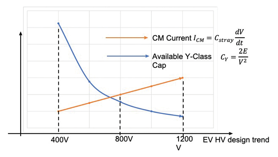
Another great challenge associated with high voltage systems is safety. EMC and safety cannot be discussed separately in an HV system. Global Technical Regulation on Electrical Vehicle Safety (EVS) [11] defines the maximum capacitor energy that may be stored in the Y-capacitors to be 0.2J. This hard limit has a profound impact of front-end input filter design of all HV modules because Y-capacitors are very effective filters for broad band noise attenuation, particularly in the lower frequency range (starting from 300kHz).
This means that when voltage level doubles, the available Y-capacitance value drops by 75% according to Equation 1:

The relationship between noise level (as represented by common-mode current) and available Y-capacitance is illustrated in Figure 2.
As the electric motor and inductors in the inverter are both inductive, higher current also means higher transient behavior caused by sudden state change. The back electromotive force (EMF) or kickback voltage caused by L·di/dt can stress or destroy components if not contained and send huge voltage spikes propagating on the HV bus line.
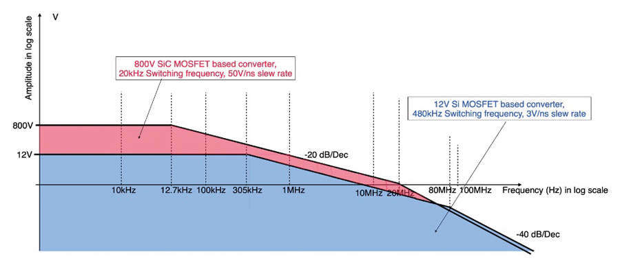
The downside of adopting wide-band-gap devices is the increase in electromagnetic interference (EMI)-related issues caused by their faster switching events. The rise time of a SiC MOSFET can be as small as a few nanoseconds, leading to a slew rate of 50-200V/ns [12].To enable such fast speed characteristics, gate drivers are equipped with short high peak pulse current features, which could also pose EMI issues.
SMPS units such as buck and boost converters in the automotive application often have a switching frequency range between 150kHz and 500 kHz. The rise and fall time of the switches can be as short as a few nanoseconds. The noise spectrum shows less energy compared with power switching devices but covers a much wider frequency range. Figure 3 demonstrates the switching noise profile between an LV buck converter and an HV inverter.
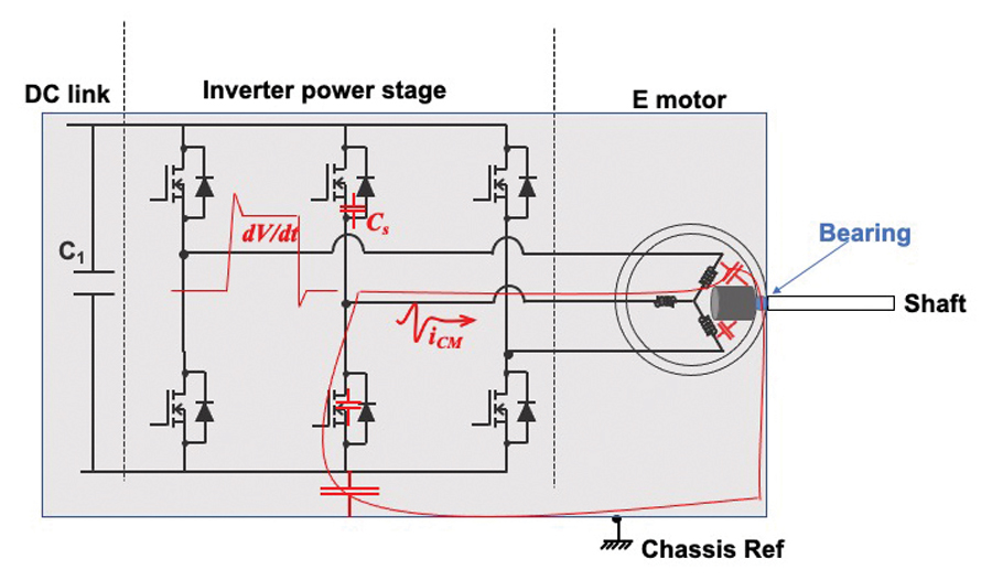
Bearings in an electric motor have moving metal balls or rollers in fixed metal shells. Very thin layers of lubricant sit between the two parts which therefore have a high capacitance and can carry high displacement currents. Because the lubricant is so thin, and because the bearings are not perfect, there can be an occasional electrical breakdown and even direct touching of the two metal parts. Therefore, the bearing current is partly capacitive, which gives a pulse of current during every switching transition and partly random high current spike [3]. This random breakdown can cause very high random peak currents that can give high quasi-peak noise in the EMI scan.
Bearing current can cause an electric motor’s bearings to deteriorate, hence reducing the lifetime of the powertrain. Bearing currents that circulate in the powertrain also cause conducted and radiated emissions, as shown in Figure 4.
In Figure 1, the term “reference” is used rather than the term “ground.” It should be noted that circuit grounds are not necessarily the same as EMC grounds. To keep it simple and clear, there can only be one EMC ground, which is the metal chassis of the unit, or what we call the RF reference. The metal enclosure of a module has contact points to the vehicle chassis (either through direct bonding or mechanical fixtures); therefore, we treat the metal enclosure as a chassis reference.
The HV-line is the HV design reference, and it should be isolated from the vehicle chassis reference (either by dielectrics or by Y-capacitors). LV designs should have 0V as the reference points, and that should be the only design reference point. The idea of splitting analog and digital ground points is based on misconceptions and is not a good design approach [16].
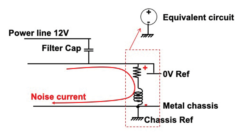
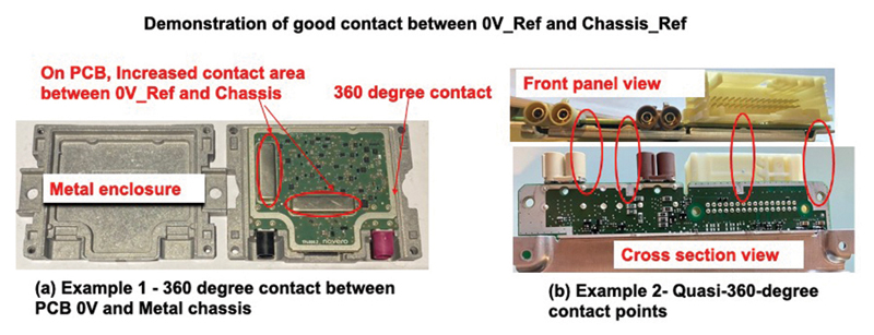
The connection between the 0V reference (either on a PCB or a connector pin) and the chassis reference will introduce inductance [16]. The RF currents will inevitably flow in those inductances, leading to noise voltages that will help drive emissions. This is shown in Figure 5. As a result, efforts to minimize the inductance of the connection should be made in the module design. Among the schemes that reduce inductances between two reference points, the most effective way is to increase direct contact areas between the 0V Ref and Chassis Ref. This is demonstrated in Figure 6. Most of the time, multiple contact points along the edges and around corners of a PCB create a quasi-360-degree contact.
There are many types of front-end filters, including the two-stage filter shown in Figure 1. In Figure 1, the L1 and C2 configuration forms the first-stage low-pass filter. The second-stage filter consists of a CMC and Y-capacitors. Notice that, together with the DC link capacitor C1, the first-stage filter effectively acts as a p (C-L-C) filter.
For powertrain applications, cores can be either used on a single power line (HV+) as an inductor or on both power lines as a CMC. It should be noted here that the designers might find CMCs such as nanocrystalline cores are not needed due to other good EMC practices in place. However, it is best to allow for Murphy’s law and to design properly from the start so that the cores can be added later if necessary [18].
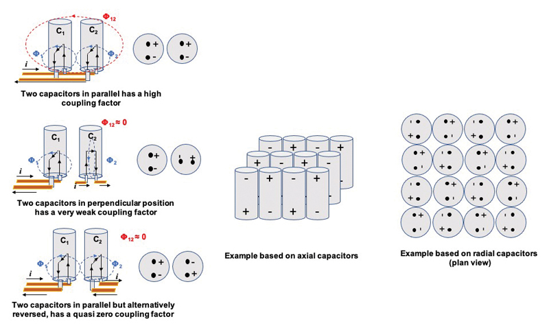
But if we arrange N-paralleled capacitors closely together, and so that they are alternately reversed or so that the self-inductance of the capacitors are in perpendicular position to each other, their magnetic fields will tend to oppose each other, canceling them out to some extent (as now mutual inductance is kept at a minimum). Since weaker fields mean lower inductances, we may be able to achieve greater than a 1/N reduction in overall self-inductance [20].
Because the common-mode current ICM can be calculated by Equation 2:


Reducing the slew rate helps to mitigate spikes or ringing, but at the cost of increased switching loss. Reducing Cstray can be achieved by selecting optimized packaging and applying good layout practice. The ringing of the switching is caused by the L-C circuit resonance, and good layout practice to achieve lower stray inductance (e.g., device connections to the bus bar) helps reduce the ringing.
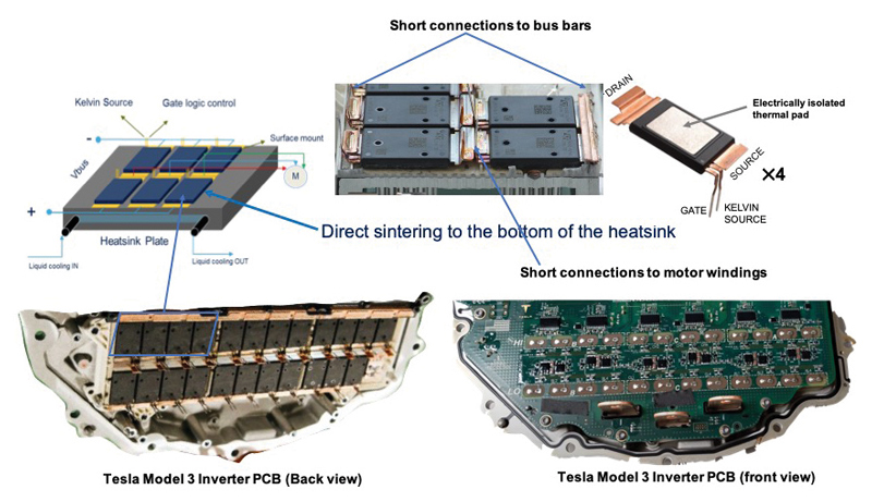
To share the large current, N SiC MOSFETs are placed in parallel. This configuration results in 1/N RDS(ON), allowing very low conduction loss. The total ESL of the devices might not be as low as 1/N for the same reason we explained when we talked about multi capacitors in parallel. However, ways of shortening the connections, such as connections between the devices and bus bars and the connections between the devices and motor windings, can minimize the inductance.
Figure 10 on page 20 demonstrates the SiC MOSFETs layout in the powertrain module of a Tesla Model 3. Four MOSFETs are put in parallel to form one switching block. Altogether, there are 24 switching devices in a very tight package space, with short connections to minimize the parasitic inductance. Direct sintering of the SiC MOSFET to the bottom of the heat sink helps remove the heat efficiently.
Techniques such as using SiC Schottky diodes in parallel to SiC MOSFETs to eliminate the reverse recovery charge effect were presented in [3]. But more manufacturers are integrating very fast and robust intrinsic body diode into the device package; hence separate antiparallel diodes are not required. Generally, locating decoupling capacitor arrays close to the switching devices is also crucial to reduce the ringing effect of the switching events.
The EMC design follows guidelines similar to those we previously discussed, which is to apply good layout practice, design front-end and output filters on both power and signal lines, and apply sufficient global and local decoupling capacitors.
CMCs are often seen in the LV power system design, and the X2Y balanced capacitor was introduced previously in this article. Although the HV (above 400V) X2Y part is not automotive qualified, there are plenty of AEC-Q200 qualified parts [19] that can be used in the control unit of a powertrain module. [21] introduced X2Y capacitor in an SMPS design.
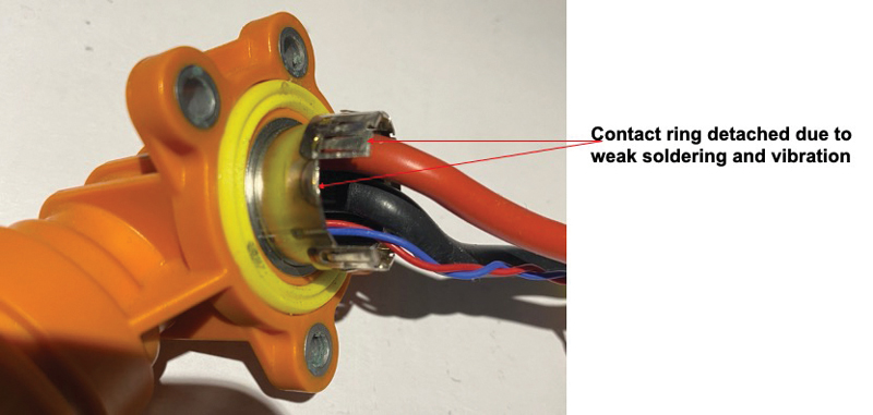
Other methods of mitigating the common-mode noise, which contributes to the shaft voltage and bearing current, are to add the common-mode filter along the motor windings. Shielded cables also help [13]. But for a compact module design, these methods are generally not considered.
Most of the techniques introduced in this article follow EMC design principles, such as reducing parasitic parameters, 360-degree shielding, and bonding. New passive components (such as nanocrystalline core and X2Y capacitors) can also be considered, as well as software schemes to mitigate the common-mode noise. By adopting these design techniques, engineers can be more confident that the powertrain module they design will pass the EMC tests, potentially even the first time around!
- J. Miller, “Plug-in hybrid vehicles face attack despite gains in range,” Financial Times Special Report – Energy Efficiency, 2020.
- Unknown, “Lightweight, compact and high-efficiency powertrain for electric vehicle EVs,” Nissan Motor Corporation, [Online]. Available: https://www.nissan-global.com/EN/TECHNOLOGY/OVERVIEW/e_powertrain.html.
- M. Zhang, “Demystifying EMC in an Electric Vehicle’s Drive Unit,” Interference Technology, 2020.
- CISPR 25:2016, 4th edition “Vehicles, boats and internal combustion engines – Radio disturbance characteristics – Limits and methods of measurement for the protection of on-board receivers,” 2016.
- H. W. K. R. (Hrsg.), Handbuch Kraftfahrzeugelektronik, ATZ/MTZ-Fachbuch, 2006.
- CISPR 36:2020, “Electric and hybrid-electric road vehicles – Radio disturbance characteristics – Limits and methods of measurement for the protection of off-board receivers below 30 MHz,” 2020.
- J551/5, “Performance Levels and Methods of Measurement of Magnetic and Electric Field Strength from Electric Vehicles, 150 KHz to 30 MHz.”
- GB/T 18387, “Limits and Test Method of Magnetic and Electric Field Strength from Electric Vehicles,” 2017.
- B. Z. X. L. Xuemei Huang, “Analysis and Verification of Magnetic Field Radiation Disturbance Standard for Electric Vehicle Below 30 MHz,” Safety and Compliance, no. 5, pp. 37‑39,55, 2020.
- Porsche, “The battery: Sophisticated thermal management, 800-volt system voltage,” [Online]. Available: https://newsroom.porsche.com/en/products/taycan/battery-18557.html.
- “Global Technical Regulation on Electric Vehicle Safety (EVS),” United Nations, 2018.
- Infineon, “CoolSIC 1200V SiC MOSFET Application Note.”
- T. Hadden et al., “A Review of Shaft Voltages and Bearing Currents in EV and HEV Motors,” IECON 2016 – 42nd Annual Conference of the IEEE Industrial Electronics Society, Florence, 2016, pp. 1578-1583.
- K. Armstrong, “EMC and Safety for Installations: Part 1,” In Compliance Magazine, October 2020, https://incompliancemag.com/article/emc-and-safety-for-installations-part-1.
- B. R. Archambeault, PCB Design for Real-World EMI Control, Norwell, Massachusetts: Kluwer Academic Publishers, 2002.
- K. Armstrong, “Advanced PCB design and layout for EMC Part 4 – Reference planes for 0V and power,” [Online]. Available: https://www.emcstandards.co.uk/files/part_4_planes_corrected_29_june_17.pdf.
- Patrick G. André and Kenneth Wyatt, EMI Troubleshooting Cookbook for Product Designers, SciTech Publishing, 2014.
- K. Armstrong, “Design Techniques for EMC Part 5 – Printed Circuit Board (PCB) Design and Layout,” [Online]. Available: http://www.compliance-club.com/pdf/128424618153773750DesignTechPart5(1st).PDF.
- Johanson Dielectrics, “EMI Filter & Decoupling Capacitors,” [Online]. Available: https://www.johansondielectrics.com/emi-filter-decoupling-capacitors.
- K. Armstrong, EMC for Printed Circuit Boards, Nutwood UK Ltd, 2010, ISBN:978-0-9555118-5-1.
- Keong Kam, David Pommerenke, Federico Centola, Cheung-wei Lam, Robert Steinfeld, “EMC Guideline for Synchronous Buck Converter Design,” in 2009 IEEE International Symposium on Electromagnetic Compatibility, Austin, TX, 2009.
- MRC, “MRC Engineering Handbook.”
- D. W. C. Terry L. Bossaller, “Kit and Method for Attaching a Grounding Ring to an Electrical Motor,” United States of America Patent US2010/0001602A1, 7 Jan 2010.
- A. M. Hava and E. Ün, “A High-Performance PWM Algorithm for Common-Mode Voltage Reduction in Three-Phase Voltage Source Inverters,” IEEE Transactions on Power Electronics, vol. 26, no. 7, pp. 1998-20089, July 2011.

