he Charged Device Model (CDM) qualification level is essentially correlated to the peak ESD discharge current [1]. Hence, several modeling approaches have been proposed to predict CDM peak current for a given package and CDM voltage level based on lumped-element equivalent circuits [2, 3]. However, the behavior of ultra-high-speed interfaces is more complex, involving fast rise time waveforms and on-die transient phenomena that cause device failure at lower CDM levels [4]. Distributed parasitics models of both on-chip circuitry and package wiring are required to capture such phenomena properly.
- Field plate to device under test (DUT) capacitor CDUT, considering the contribution of package conductors and on-die traces.
- Ground plane to DUT capacitor CDG, always significantly smaller than CDUT.
- Ground plane to field plate capacitor CFG, including the chassis contribution (separated in more complex 5-capacitor models [3]).
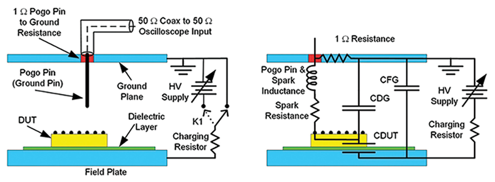
- The DUT is modeled as a lumped capacitor CDUT. This approach is suitable for peak current estimation but does not allow the evaluation of the actual voltage at the pad and the voltage drop on internal nodes (critical for deeply scaled, overshoot-sensitive technologies).
- With respect to the model shown in Figure 1, package trace and bonding impedance are modeled as a lumped RL series (Rpkg, Lpkg). However, the actual discharge channel behavior is more complex than an RL series, with reflections and delays that may affect the input waveform.
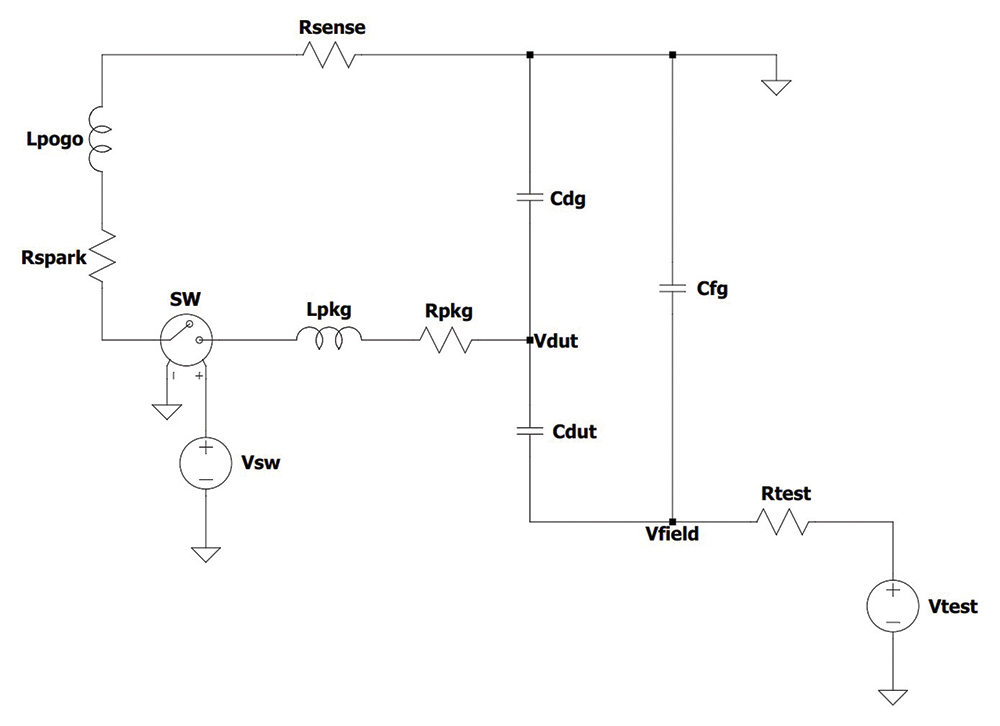
To account for the package trace behavior at fast transients as well, the lumped Rpkg and Lpkg need to be replaced by a more accurate channel model, capturing fast rise time slopes and possible reflections. Since the channel behavior strongly depends on the topology and layout of the substrate wiring, the most accurate modeling approach will require S-parameter extraction through calibrated EM simulations. However, a simple lossy transmission line (TL) already represents a good trade-off between accuracy and complexity, which can be included in the Spice model.
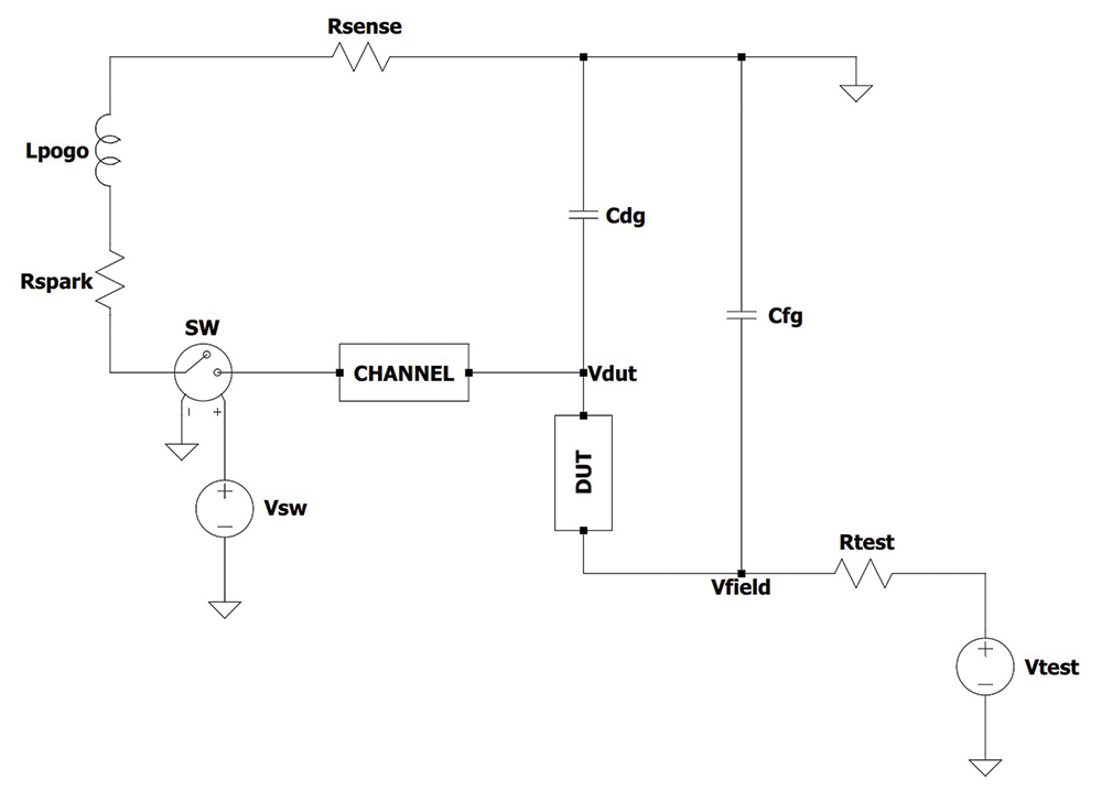
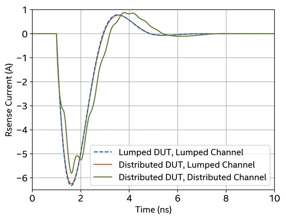
Figure 4 shows the comprehensive CDM tester model with two building blocks representing the distributed DUT model and the distributed discharge channel model (S-parameter or lossy TL).
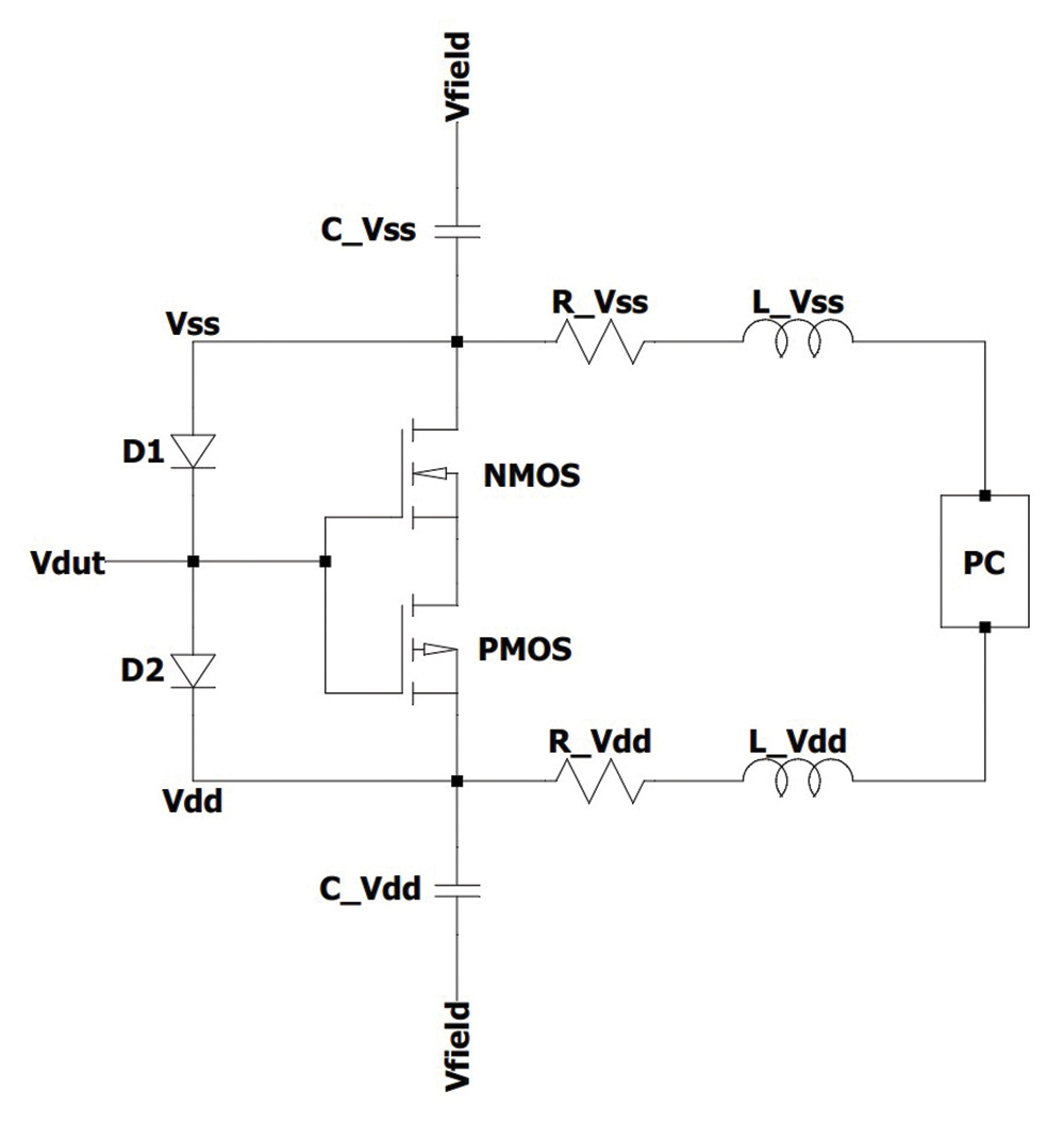
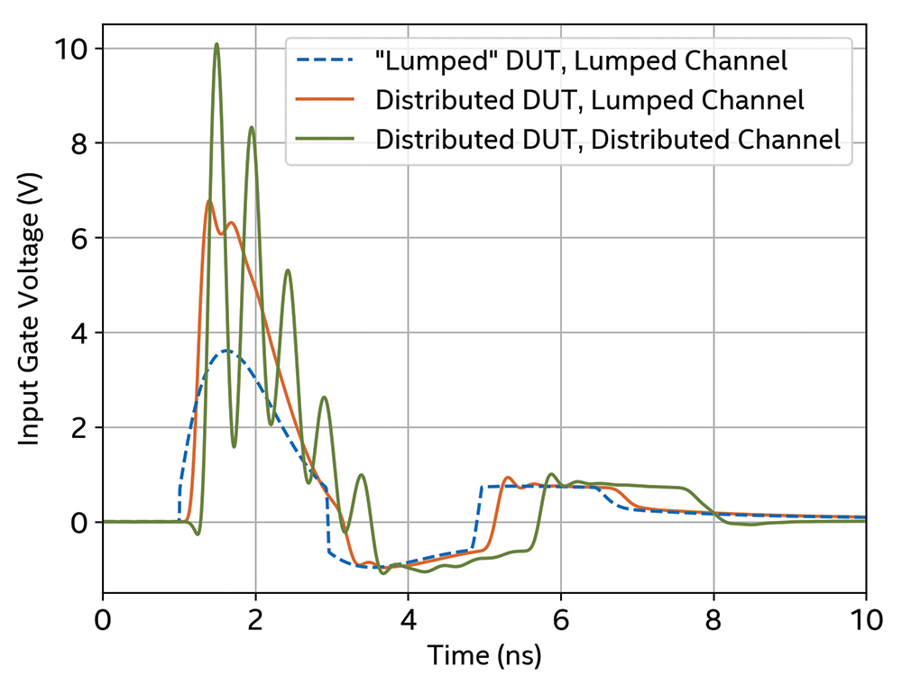
The voltage waveform at the input gate oxide can only be evaluated in the presence of a distributed DUT model. Hence, the following cases are considered in Figure 6:
- To model the voltage without on-die parasitics, a distributed DUT model with no inductance and resistance contributions on Vdd and Vss branches is considered. This yields the smooth voltage waveform indicated as “lumped” DUT (blue dashed curve) with a low peak voltage below 4V.
- The presence of on-die parasitic resistance and inductance in the distributed DUT model leads to an additional voltage drop and increases the peak voltage to more than 6 V at the input gate oxide (orange curve).
- More severe voltage spikes up to 10 V are obtained by adding the distributed channel model on top (green curve).
- ANSI/ESDA/JEDEC JS-002-2022, “Joint Standard for Electrostatic Discharge Sensitivity Testing – Charged Device Model (CDM) – Device Level.” http://www.esda.org/standards/esda-documents
- Shukla, Vrashank, et al., “Predictive Modeling of Peak Discharge Current During Charged Device Model Test of Microelectronic Components,” 2013 35th Electrical Overstress/Electrostatic Discharge Symposium, IEEE, 2013.
- Atwood, Bruce C., et al., “Effect of Large Device Capacitance on FICDM Peak Current,” 2007 29th Electrical Overstress/Electrostatic Discharge Symposium (EOS/ESD), IEEE, 2007.
- Ishfaq, Umair, et al., “Advanced CDM Simulation Methodology for High-Speed Interface Design,” 2022 44th Annual EOS/ESD Symposium (EOS/ESD), IEEE, 2022.