his column describes the operation of an ideal difference amplifier. First, the input-output relationship for the generic input voltages is derived. Subsequently, the differential mode and common mode voltages are introduced. Then, the difference amplifier driven by the common mode and differential mode input voltages is analyzed. It is shown that an ideal difference amplifier (with no resistance mismatches) eliminates the common mode portion of the input voltage and amplifies only the differential mode portion of the input voltage.
or
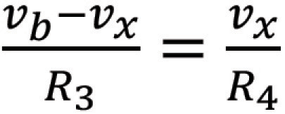
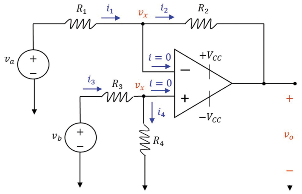
From Eq. (1.2a) we obtain
while from Eq. (1.2b) we get
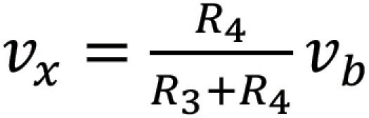
Substituting Eq. (1.3b) into Eq. (1.3a) we get
or
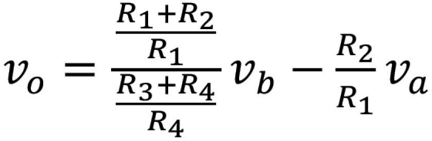
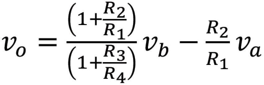
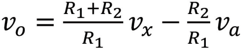
which is equivalent to
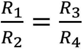
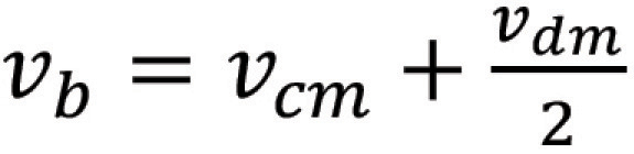
when
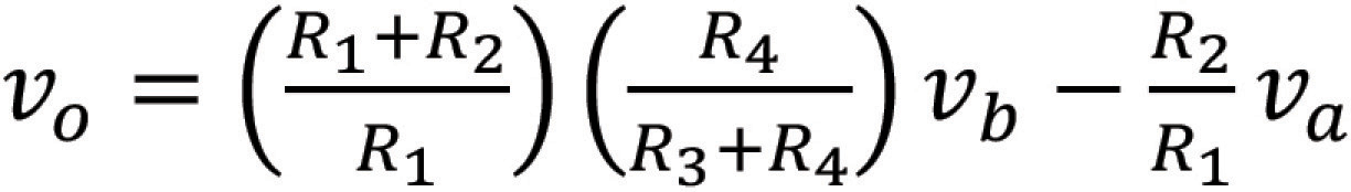
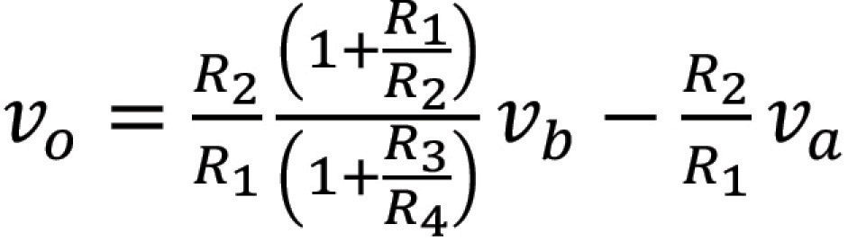
the relationship in Eq. (1.7) becomes
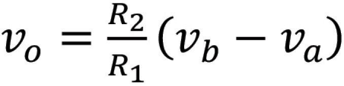
which describes the input-output relationship of the difference amplifier.
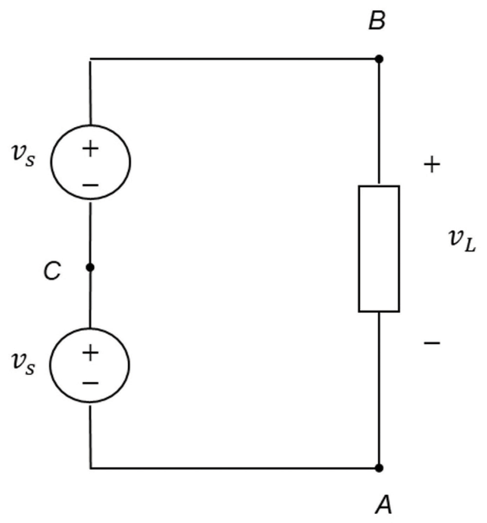
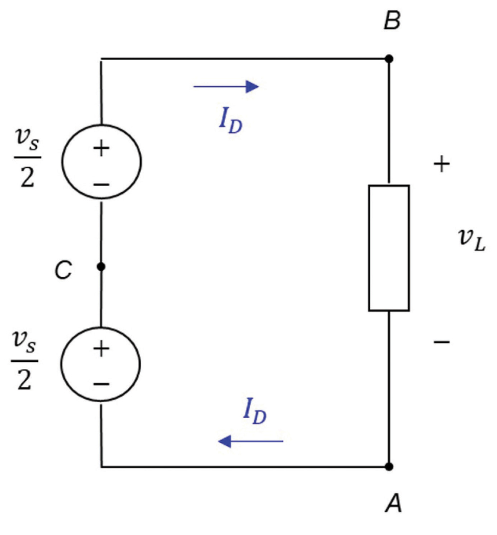
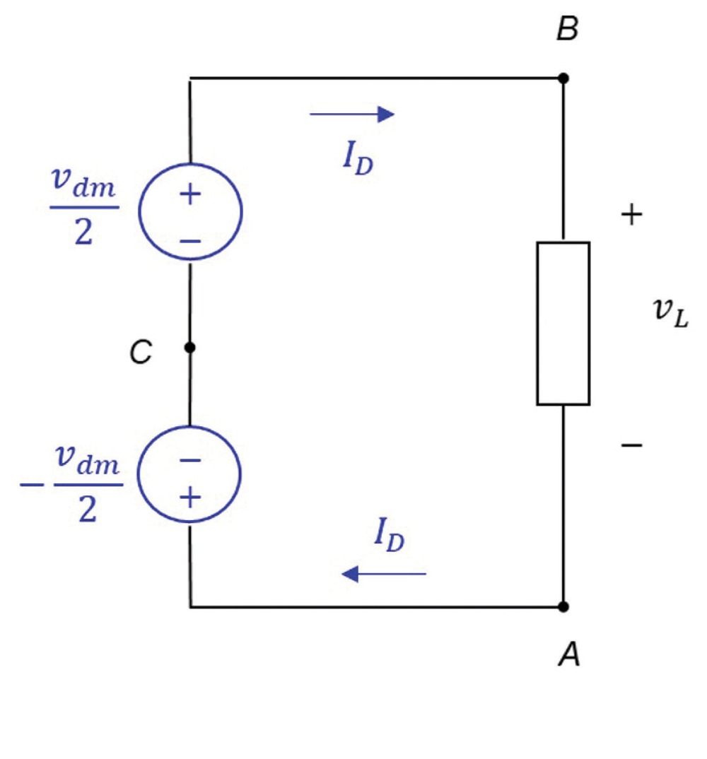
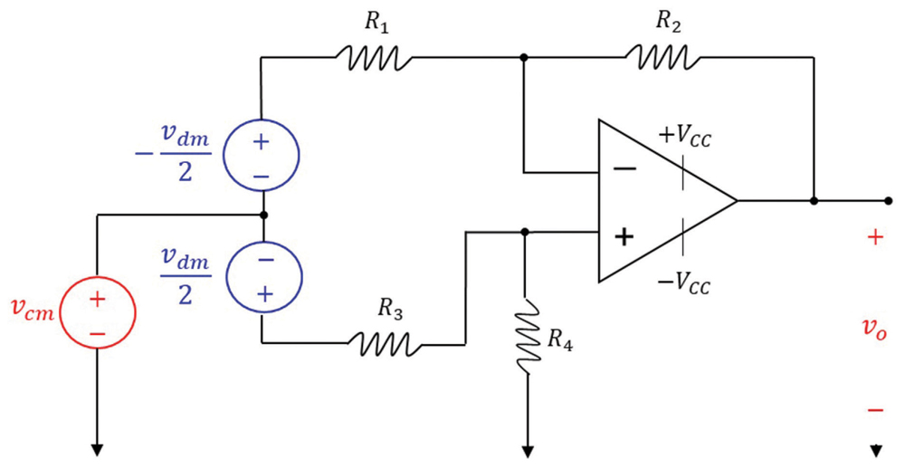
Circuit 2, shown in Figure 3, is equivalent to the one in Figure 4, where the polarity and value of the lower source have been reversed, and the names of the sources have been changed from vs to vdm to emphasize that these are differential mode sources.
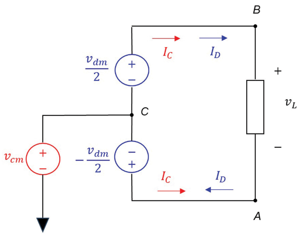
This common-mode source injects the common-mode current, IC, into the forward and return path, as shown in Figure 5.

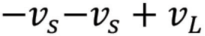
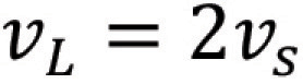
Thus

or

leading to

or
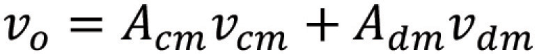
Equations (3.4) and (3.5) express the output of the difference amplifier in terms of the common mode and differential mode input voltages.
when
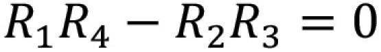
we have
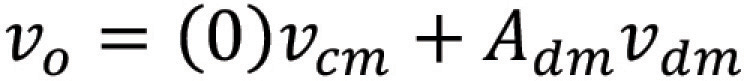
Thus, an ideal difference amplifier (with no resistance mismatches) eliminates the common mode portion of the input voltage and amplifies only the differential mode portion of the input voltage.
References
- James W. Nilsson and Susan A. Riedel, Electric Circuits, Pearson, 2015.
- Bogdan Adamczyk, Foundations of Electromagnetic Compatibility with Practical Applications, Wiley, 2017.