his is the first of several columns investigating the effectiveness of decoupling capacitors while varying the topology of vias, trace length between the decoupling capacitor and the integrated circuit (IC) power/ground pins, and distance from the internal power and ground plane pair. Specifically, the impact of the PCB geometry will be evaluated by performing RF Emission testing on six PCB variants, according to the CISPR 25 standard. Part 1 of this study defines the board topologies and the PCB circuitry. The following parts will show the RF Emissions results.


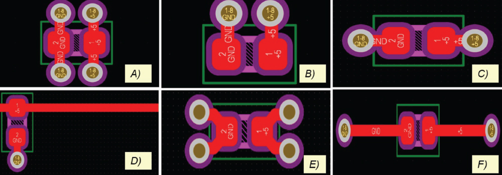
Board B was similar to Board A but had only two vias connected to the capacitor instead of four. The via leading to the internal power plane was placed 0.03 inches above the capacitor’s power pin, while the via leading to the internal ground plane was placed 0.03 inches above the capacitor’s ground pin. Again, there was 0.03 inches of separation between the power via and the ground via.
Board C had two vias connected to the capacitor, where one was approximately 0.026 inches to the left of the capacitor’s ground pin, and the other was 0.025 inches to the right of the capacitor’s power pin. 0.085 inches separated the vias from each other.
Board E had four vias connected to the capacitor. Each via was placed at a vertical distance of approximately 0.015 inches and a horizontal distance of approximately 0.026 inches from the center of the respective capacitor pin. This left 0.086 inches of distance between each power and ground via pair. The traces connecting the vias to the capacitor pin pads were also curved.
Board F was similar to Board C but had a longer trace between each via and the capacitor. Each via was approximately 0.1 inches from the center of its respective capacitor pin pad, making the distance between the vias 0.234 inches.

Ground planes had no pullback distance from the board edges, while the power plane was pulled back a distance of 20H, with H being the thickness of the core.