SD protection devices designed to safeguard sensitive high-speed interfaces must meet stringent signal integrity requirements. As bandwidth demand increases, these devices require increasingly lower capacitance, as shown in Figure 1. However, with the rise of high-speed applications like HDMI 2.2 and USB 4, ESD solutions should not only have smaller capacitance but must also be designed with robust signal integrity practices to ensure compliance with stringent performance standards.

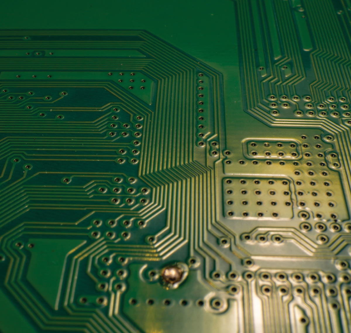
Currently, most manufacturers of discrete ESD protection devices measure S-parameters of their devices using test PCBs compatible with 4-port Z-probes, or directly on the device using ACP probes for 2-pin devices. It is well understood that the design and quality of the measurement of a PCB can impact the signal integrity performance of the device under test (DUT). However, in many cases, these measurement PCBs are not specifically optimized for high frequency or RF performance, which can compromise the accuracy of the results.
In this article, we explore the impact of the measurement PCB on S-parameter characterization by examining ESD protection devices with two different capacitance values. We demonstrate how the PCB can affect the accuracy of the high-frequency measurements, particularly as device capacitance enters low femtofarad range. To better predict these effects, we utilize 3D electromagnetic (EM) simulations to model the device along with the measurement PCB. The simulations are validated through direct comparison to measurements, highlighting the importance of simulation-driven design and verification in ensuring accurate characterization of ESD devices.
Furthermore, integrating both functions into a single package significantly reduces the board space and minimizes package parasitics. This reduction in package parasitics helps lower the inductance and capacitance of the overall device, thereby increasing its differential bandwidth.
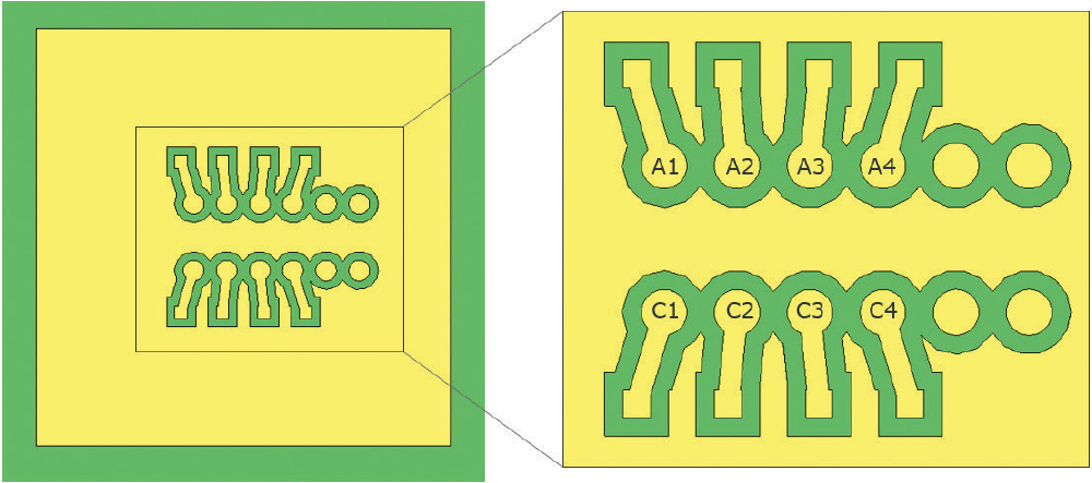
PCMF devices are offered in package variants that support one, two, or three differential channels, as illustrated in Figure 3. This range of configurations provides designers with flexible protection options tailored to a wide variety of high-speed interface applications. An example of a PCB used to measure the S-parameters of the PCMFs is shown in Figure 4. This PCB is most ideal to measure the three-channel protection PCMF. But it can also be used for measuring one- and two-channel protection devices.

When we use a standard impedance trace calculator to estimate the impedance of the PCB traces, it may show that the characteristic impedance of the PCB lines is around 50 Ohms, as they typically assume uniform trace lengths and consistent spacing to the ground. But they do not count for the impedance discontinuity when the spacing to the ground plane is varied, which can lead to signal reflections and increased insertion loss, effects that are difficult to estimate from traditional calculations or simple equivalent circuit simulations.
To address this, 3D electromagnetic (EM) simulations offer a powerful and efficient way to model the complete PCB structure, including all geometric and material complexities.
For these simulations, we utilize a powerful tool for high-frequency 3D EM modelling.[1] To ensure accurate correlation between simulation and measurement, the PCB used for measurement is also included in the simulation environment. This allows for a realistic representation of the measurement setup, including all parasitic effects introduced by the board.
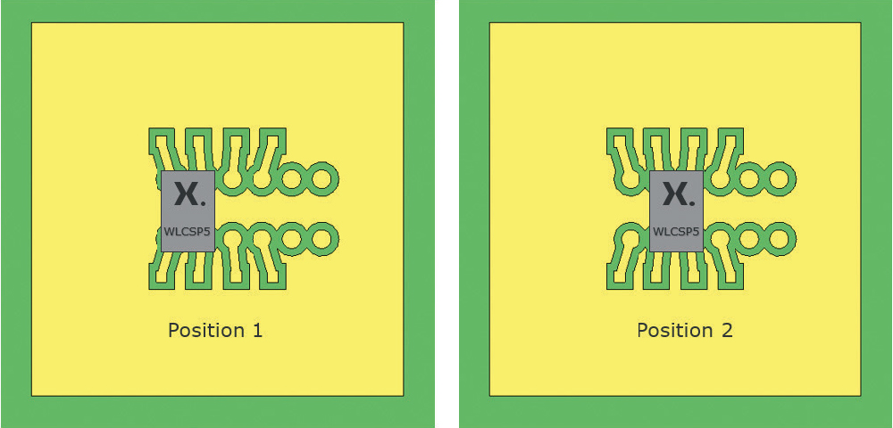
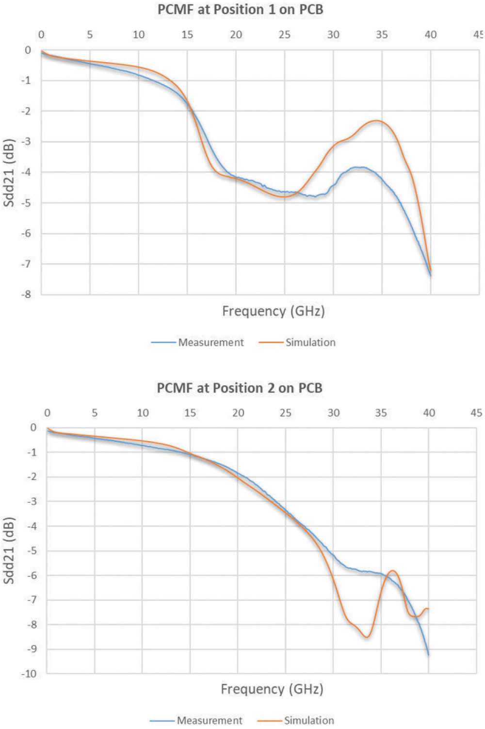
The differential insertion loss of a PCMF device (referred to as PCMFa) is simulated in position 1 and position 2 of the measurement PCB, which are shown in Figure 5. The simulation results are compared to measurements as shown in Figure 6. The correlation between simulation and measurement is quite good up to 30GHz, demonstrating the accuracy and reliability of the modelling approach.
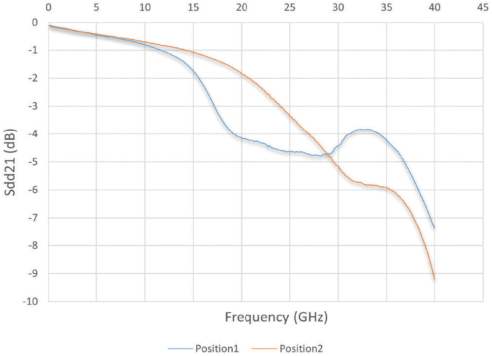
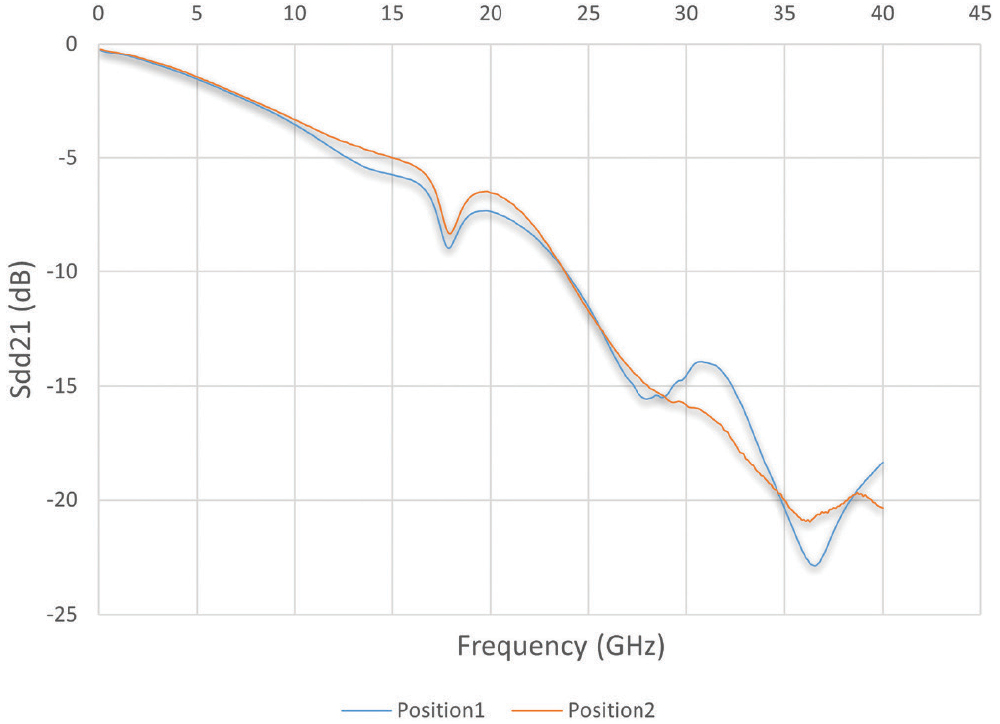
When we measure a different PCMF, PCMFb, which has nearly two times higher inductances of the common mode filters and capacitance of the ESD diodes, the influence of the PCB becomes less significant. As shown in Figure 8, the differential insertion loss for PCMFb exhibits much smaller variation between the two measurement positions. This indicates that the device’s intrinsic electrical characteristics dominate its performance, making it less sensitive to the measurement PCB.
Through measurements and 3D EM simulations, we have shown that variations in PCB layout, such as trace asymmetry and inconsistent spacing to the ground plane, can significantly affect the performance of ESD protection devices, especially those with capacitance in the femtofarad range. The use of advanced simulation tools enables designers to model these effects with more accuracy, allowing for better prediction and optimization of device behavior in real-world conditions.
Ultimately, this article underscores the importance of co-designing ESD protection devices and their measurement environments. By combining accurate modelling, careful PCB design, and robust measurement practices, engineers can ensure that ESD protection solutions meet the stringent demands of today’s high-speed digital systems.
- CST Studio Suite by Dassault Systèmes, 05 June 2025.